kicad-learning-path
KiCad Learning Path




My hands-on journey from complete beginner to advanced electronics and PCB design with KiCad, built from small, simple circuits. Every project teaches one new idea and is documented with schematics, calculations, timing diagrams, layout rules, verification reports and manufacturing files.
Table of contents
- About this repository
- Learning approach
- Projects so far
- Roadmap
- Coverage by track
- Components index
- What every project includes
- Repository structure
- Tools
- How to open a project
- Feedback
- License
About this repository
This repository documents my path through electronics and PCB design. I build one small circuit at a time, calculate it by hand, design it in KiCad, check it with ERC and DRC, prepare the manufacturing files, and write down what I learned.
The projects are ordered so that each one builds on the last. If you are learning too, start at Project 1 and work forward. The complete plan, with the components and ideas of every project, is in ROADMAP.md.
Learning approach
| Rule | Why |
|---|---|
| One new idea per board | So you can see exactly what each component does |
| About 12 parts or fewer | Small enough to understand every connection |
| Through-hole parts and 0805 SMD only | Hand-solderable, no special equipment |
| 2-layer board, standard KiCad libraries | Cheap to build and easy to reproduce |
| Calculate first, then build, then measure | Theory is checked against reality |
| Timing or waveform diagram wherever signals change over time | Turns formulas into something you can verify on an oscilloscope |
Projects so far
| # | Project | Preview | What it teaches | Documentation |
|---|---|---|---|---|
| 1 | LED + Push-Button | 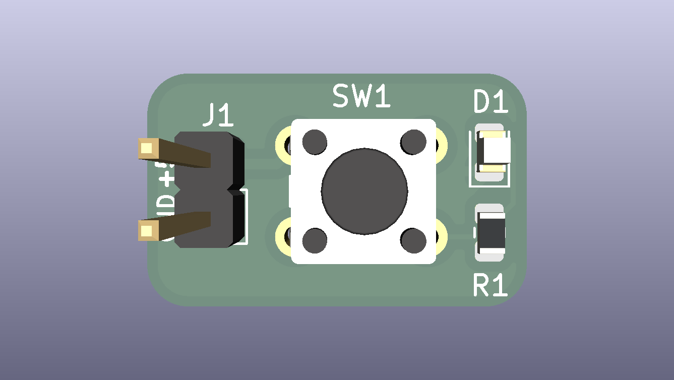 |
Ohm’s law, LED current limiting, resistors and switches, the full KiCad workflow, Gerber export | README · Design notes |
| 2 | 555 LED Blinker | 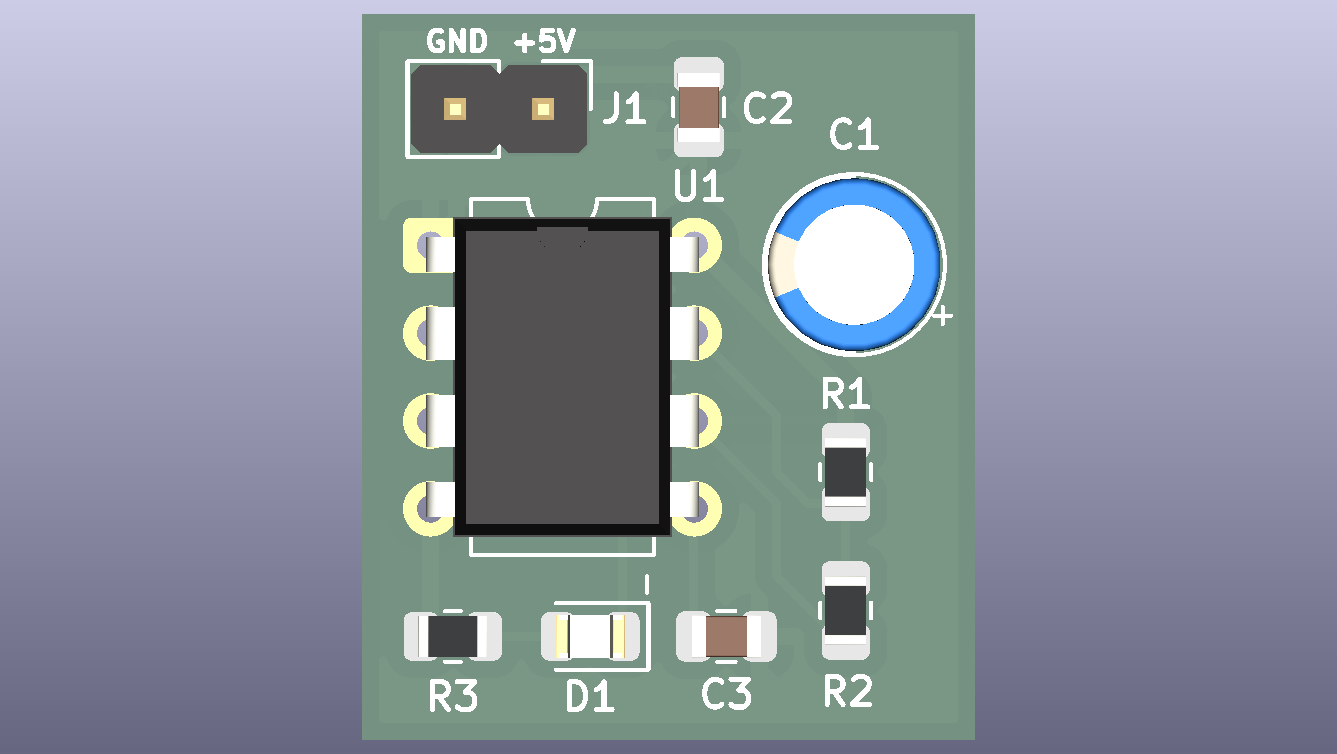 |
Capacitors, RC time constant, the 555 timer, decoupling, ground pours and vias, timing diagram | README · Design notes |
| 3 | Voltage Divider, Potentiometer and Light Sensor | 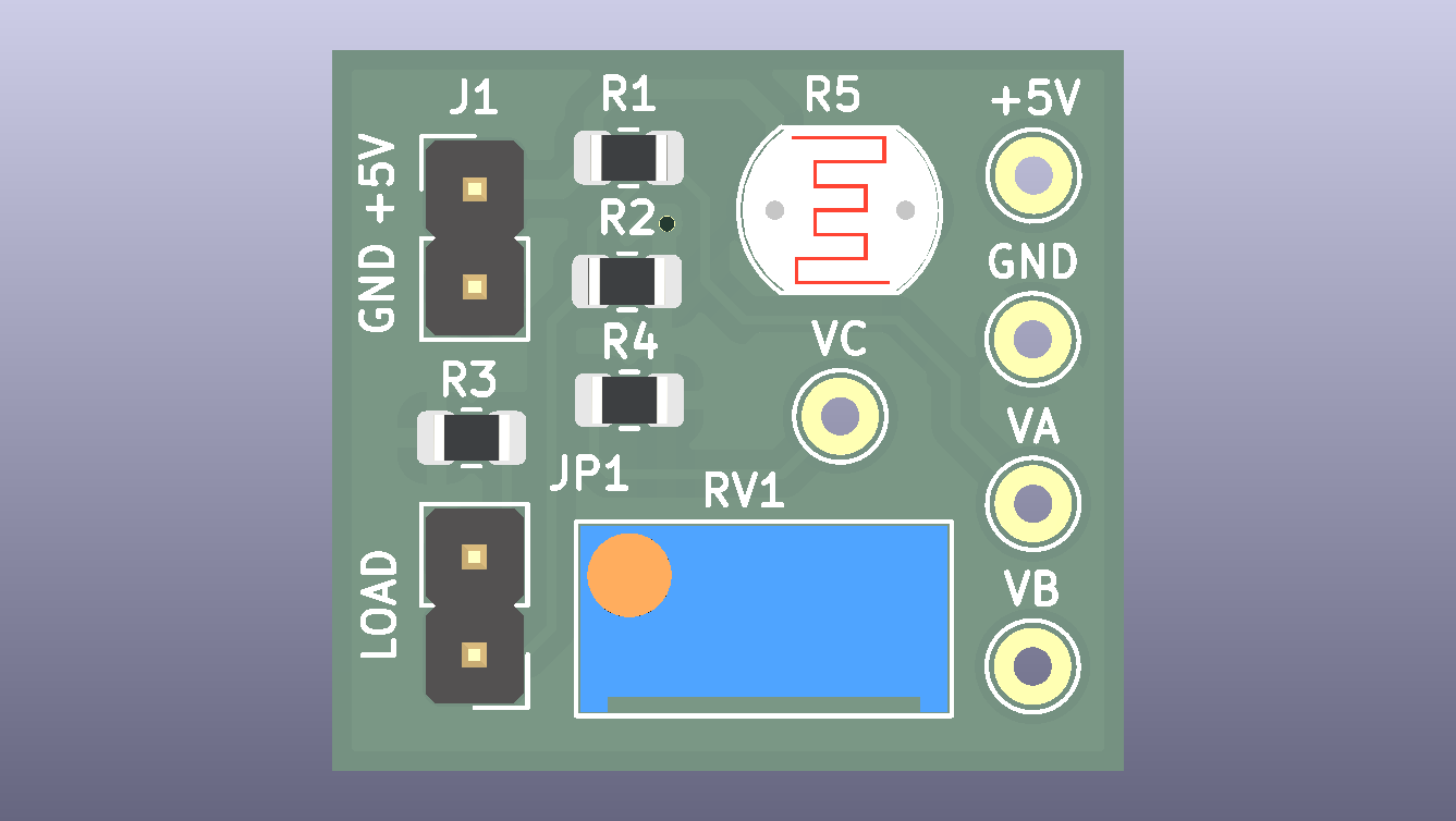 |
The voltage divider formula, the loading effect, potentiometer, LDR light sensor, test points, transfer curves | README · Design notes |
| 4 | NPN Transistor Switch | 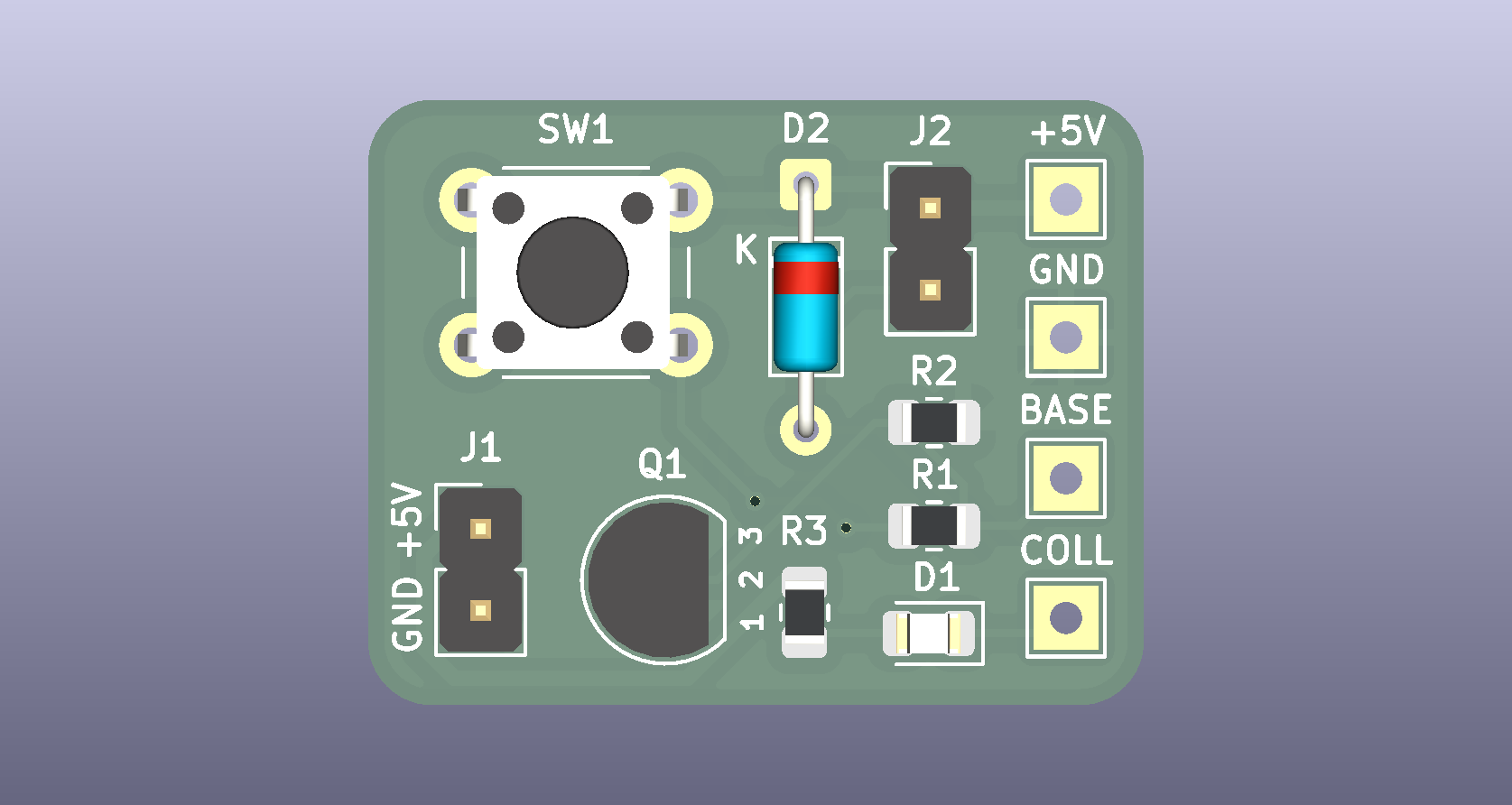 |
The transistor as a switch, base resistor and saturation, flyback diode, net classes, switching waveform | README · Design notes |
| 5 | Diode Power Entry and 5 V Linear Regulator | 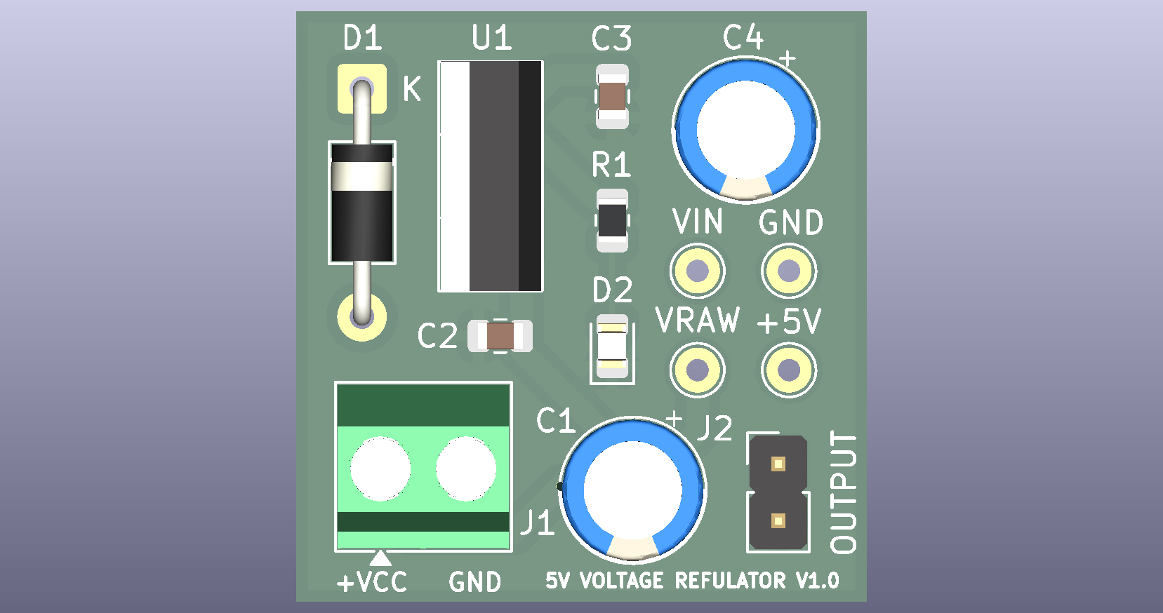 |
Reverse-polarity protection, linear regulation and dropout, heat and heatsinks, input and output capacitors, voltage and power budget | README · Design notes |
Roadmap
Fifteen simple circuits, from the first resistor to a complete microcontroller board.
| # | Project | Level | Track | Key ideas | Status |
|---|---|---|---|---|---|
| 1 | LED + Push-Button | Beginner | Basics | Resistor, LED, switch, Ohm’s law | Done |
| 2 | 555 LED Blinker | Beginner | Timing | Capacitor, timer IC, RC timing, decoupling | Done |
| 3 | Voltage Divider, Potentiometer and Light Sensor | Beginner | Analog | Divider formula, loading effect, LDR, test points | Done |
| 4 | NPN Transistor Switch | Beginner | Analog and power | BJT, base resistor, flyback diode, saturation | Done |
| 5 | Diode Power Entry and 5 V Linear Regulator | Beginner | Power | Reverse-polarity protection, regulator, heat dissipation | In progress |
| 6 | RC Low-Pass Filter | Intermediate | Analog | Cutoff frequency, step response, frequency response | Planned |
| 7 | Op-Amp Buffer and Amplifier | Intermediate | Analog | Feedback, gain, single-supply operation | Planned |
| 8 | Comparator Night-Light | Intermediate | Analog to digital | Comparator, hysteresis, sensor to switch | Planned |
| 9 | Logic Gates Trainer | Intermediate | Digital | 74HC gates, truth tables, logic levels, pull-downs | Planned |
| 10 | Switch Debouncer and D Flip-Flop | Intermediate | Digital | Contact bounce, SR latch, clocked memory | Planned |
| 11 | LED Chaser (555 + Decade Counter) | Advanced | Digital | Counters, clocking, sequential logic | Planned |
| 12 | MOSFET Load Switch and PWM Dimmer | Advanced | Power and analog | N-MOSFET, gate drive, PWM duty cycle | Planned |
| 13 | Buck Converter | Advanced | Power | Inductor, switching regulator, efficiency, loop layout | Planned |
| 14 | Digital Counter with 7-Segment Display | Advanced | Digital | Counter and decoder IC, display driving | Planned |
| 15 | Microcontroller Starter Board (ATtiny) | Advanced | Digital, analog and power | MCU, programming header, reset, ADC input | Planned |
Status: Done = built, verified and documented. In progress = designed or being documented. Planned = not started. The plan may be adjusted as I learn.
Coverage by track
| Track | Projects |
|---|---|
| Analog | 3, 4, 6, 7, 8, 12, 15 |
| Digital | 2, 9, 10, 11, 14, 15 |
| Power | 4, 5, 12, 13, 15 |
Components index
| Component | First used in |
|---|---|
| Resistor, LED, push-button | Project 1 |
| Capacitor (ceramic and electrolytic), 555 timer | Project 2 |
| Potentiometer, light-dependent resistor | Project 3 |
| NPN transistor | Project 4 |
| Diode, linear voltage regulator | Project 5 |
| Op-amp | Project 7 |
| Comparator | Project 8 |
| Logic gates | Project 9 |
| Flip-flop | Project 10 |
| Counter | Project 11 |
| MOSFET | Project 12 |
| Inductor, switching regulator | Project 13 |
| Decoder and 7-segment display | Project 14 |
| Microcontroller | Project 15 |
What every project includes
- README: overview, specifications, images, bill of materials, netlist, testing and status
- Design notes: electronics theory, step-by-step calculations with worst-case analysis, KiCad configuration, layout rules and the reasons for them
- Timing or waveform diagram wherever signals change over time
- Verification: saved ERC and DRC reports and a Gerber viewer check
- Manufacturing files: Gerbers, drill files and BOM, ready for a low-cost fab
- Test procedure: expected measurements to compare against the real board
Repository structure
kicad-learning-path/
├── README.md                    this index
├── ROADMAP.md                   the full 15-project plan
├── LICENSE
├── .gitignore
├── 01-led-button/
│   ├── README.md
│   ├── 01_led_button.kicad_pro / .kicad_sch / .kicad_pcb
│   ├── fabrication/             Gerbers, drill files, BOM
│   └── docs/                    design notes, schematic PDF, images, reports
├── 02-555-blinker/
│   ├── README.md
│   ├── 02_555_blinker.kicad_pro / .kicad_sch / .kicad_pcb
│   ├── fabrication/             Gerbers, drill files, BOM
│   └── docs/                    design notes, schematic PDF, timing diagram, images, reports
├── 03-voltage-divider/
│   ├── README.md
│   ├── 03_voltage_divider.kicad_pro / .kicad_sch / .kicad_pcb
│   ├── fabrication/             Gerbers, drill files, BOM
│   └── docs/                    design notes, schematic PDF, transfer curves, response diagram, images, reports
├── 04-npn-transistor-switch/
│   ├── README.md
│   ├── 04_npn_transistor_switch.kicad_pro / .kicad_sch / .kicad_pcb
│   ├── fabrication/             Gerbers, drill files, BOM
│   └── docs/                    design notes, schematic PDF, switching waveform, saturation curve, images, reports
├── 05-linear-regulator/
│   ├── README.md
│   ├── 05_linear_regulator.kicad_pro / .kicad_sch / .kicad_pcb
│   ├── fabrication/             Gerbers, drill files, BOM
│   └── docs/                    design notes, schematic PDF, operating area, power budget, images, reports
└── 06-... to 15-...             added as each project is completed
Naming: project folders are NN-short-name/ and the KiCad files inside are NN_short_name.*.
Every project folder follows the same layout:
NN-short-name/
├── README.md
├── NN_short_name.kicad_pro / .kicad_sch / .kicad_pcb
├── fabrication/
│   ├── gerbers/
│   ├── NN_short_name_gerbers.zip
│   └── bom.csv
└── docs/
    ├── DESIGN_NOTES.md
    ├── schematic.pdf
    ├── images/
    └── reports/
Tools
| Tool | Version |
|---|---|
| KiCad | 10.x |
| Libraries | Standard KiCad libraries only |
| Target fab | Low-cost 2-layer service (for example JLCPCB) |
| Gerber check | KiCad Gerber Viewer or any third-party viewer |
| Version control | Git and GitHub |
How to open a project
- Install KiCad.
- Clone or download this repository.
- Open the
.kicad_profile inside any project folder.
Feedback
Spotted a mistake in a calculation, or have a suggestion for a better layout or a simpler explanation? Please open an issue. Corrections are welcome.
License
Released under the MIT License.
Author: Nitish Ghadage · GitHub