kicad-learning-path
Voltage Divider, Potentiometer and Light Sensor


Three analog voltage dividers on one 5 V board: a fixed divider with a switchable load, a potentiometer, and a light-dependent resistor. Five test points make every voltage easy to measure. Project 3 of my KiCad learning path: the voltage divider formula, the loading effect, the potentiometer and the LDR.
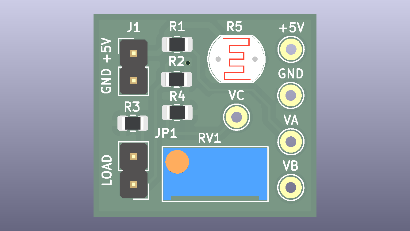
Table of contents
- Overview
- Key specifications
- Gallery
- Transfer curves and response
- How the circuits work
- Design calculations (summary)
- Purpose of each component
- Bill of materials
- Netlist
- Repository structure
- Getting started
- Testing
- Verification status
- Future improvements
- License
Overview
Projects 1 and 2 produced outputs you could see: an LED that lit and an LED that blinked. This board produces voltages you measure with a multimeter. It teaches the most useful circuit in electronics, the voltage divider, in three forms:
| Section | Circuit | What it demonstrates |
|---|---|---|
| A | Fixed divider R1 / R2, with a load R3 switched in by jumper JP1 |
The divider formula, and how a load pulls the output down (the loading effect) |
| B | Potentiometer RV1 across the supply |
A variable divider, and how the wiper position sets the output |
| C | Light-dependent resistor LDR1 and R4 |
Turning a changing resistance into a changing voltage |
New ideas compared with Project 2:
- The voltage divider formula and its Thevenin equivalent
- The loading effect, and why measuring a circuit can change it
- A three-terminal potentiometer
- A sensor whose resistance depends on light (power-law behaviour)
- Test points for measurement
- A jumper to change the circuit without soldering
- Silkscreen graphics to group sections on the board
The full engineering write-up (theory, derivations, KiCad configuration, layout rules, test procedure) is in docs/DESIGN_NOTES.md.
Key specifications
| Parameter | Value |
|---|---|
| Supply voltage | 5 V DC via J1 |
Section A output VA (TP3) |
2.50 V unloaded, 1.67 V with JP1 fitted |
Section B output VB (TP4) |
0 V to 5 V, set by RV1 |
Section C output VC (TP5) |
about 0.05 V in the dark, about 2 V at 10 lux, about 3.6 V at 100 lux (typical) |
| Supply current | about 0.95 mA typical, 1.29 mA maximum |
| Board layers | 2 |
| Board thickness | 1.6 mm |
| Copper weight | 1 oz (35 µm) |
| Board size | 70 × 40 mm |
| Components | 13 (8 circuit parts and 5 test points) |
| Pads / nets | 22 / 6 |
| Design tool | KiCad 10.0.x |
| ERC / DRC | 0 errors / 0 errors |
Gallery
Schematic
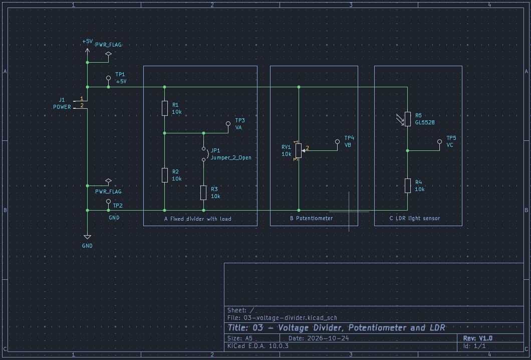
Full-size PDF: docs/schematic.pdf
PCB layout
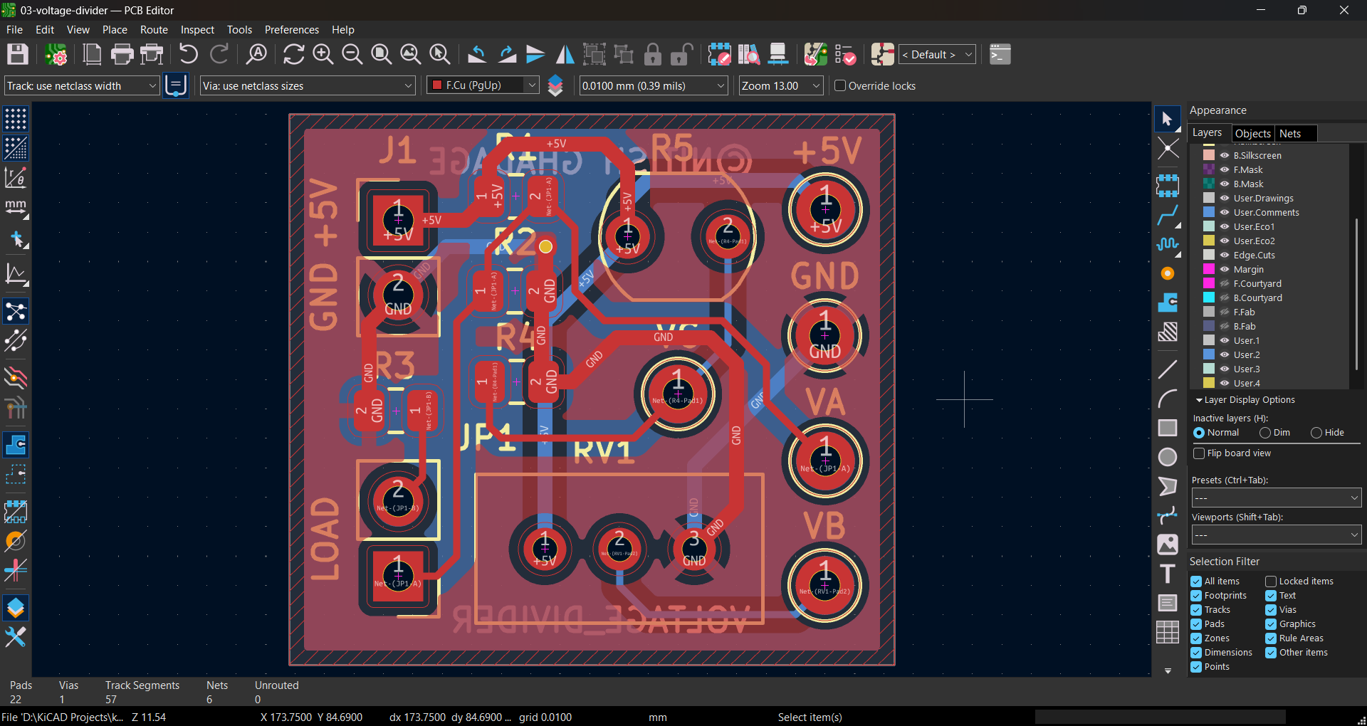
3D views
| Top | Bottom |
|---|---|
|
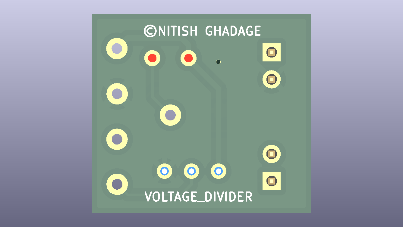 |
Transfer curves and response
Transfer curves
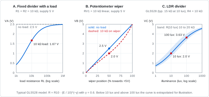
| Plot | What it shows |
|---|---|
| A. Fixed divider | The output falls as the load resistance falls. With a 10 kΩ load (JP1 fitted) it drops from 2.50 V to 1.67 V |
| B. Potentiometer | A straight line from 0 V to 5 V when unloaded. A 10 kΩ load on the wiper bends the curve (2.0 V instead of 2.5 V at mid-travel) |
| C. LDR divider | Output rises with light on a log scale. The shaded band is the part-to-part spread of the LDR (10 kΩ to 20 kΩ at 10 lux) |
LDR response in time
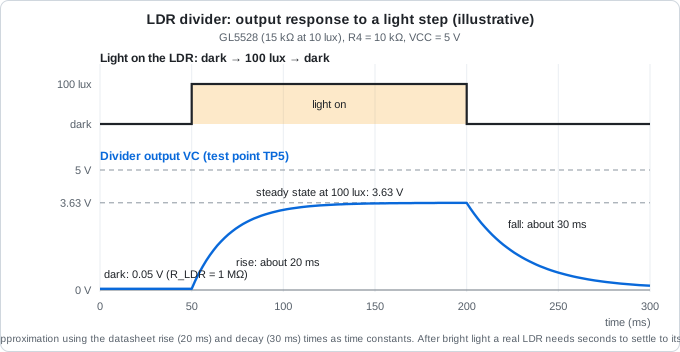
When the light changes, the LDR follows with a lag of tens of milliseconds (datasheet: about 20 ms rising, 30 ms falling), so VC rises and falls smoothly rather than instantly. After bright light the real part can take seconds to settle back to its dark value. This diagram is an illustrative first-order approximation.
How the circuits work
 +5V ──┬──────────────┬──────────────────┬──────────────┐
       R1 10k         │                  LDR1           │
       │              RV1 10k            │               │
 VA ───┼── JP1 ─ R3   │◄── wiper = VB    VC ──┬── TP5    │
       │         10k  │                       R4 10k     │
       R2 10k         │                       │          │
 GND ──┴──────────────┴───────────────────────┴──────────┘
A. Fixed divider. R1 and R2 form a series loop, so the same current flows through both. The output between them is the share of the supply that falls across R2. Fitting a shunt on JP1 connects R3 in parallel with R2, which lowers the lower half of the divider and pulls VA down.
B. Potentiometer. The two ends of RV1 connect to +5V and GND. The wiper touches the track at an adjustable point and picks off the voltage there, so turning the shaft sweeps VB smoothly from 0 V to 5 V.
C. LDR divider. In the light the LDR’s resistance is low, so most of the supply falls across R4 and VC is high. In the dark the LDR’s resistance is very high, so most of the supply falls across the LDR and VC is low.
Design calculations (summary)
Voltage divider:
\[V_{out} = V_{in} \times \frac{R_2}{R_1 + R_2} \qquad V_A = 5.0\ \text{V} \times \frac{10\ \text{k}\Omega}{10\ \text{k}\Omega + 10\ \text{k}\Omega} = 2.50\ \text{V}\]Loading effect (a load $R_L$ in parallel with $R_2$):
\[V_{A,loaded} = V_{in} \times \frac{R_2 \parallel R_L}{R_1 + (R_2 \parallel R_L)} = 5.0\ \text{V} \times \frac{5\ \text{k}\Omega}{10\ \text{k}\Omega + 5\ \text{k}\Omega} = 1.67\ \text{V}\]Potentiometer (wiper at fraction $x$ of the travel, unloaded):
\[V_B = V_{in} \times x\]LDR divider (LDR on the supply side):
\[V_C = V_{in} \times \frac{R_4}{R_4 + R_{LDR}} \qquad R_{LDR}(E) = R_{10}\left(\frac{E}{10\ \text{lux}}\right)^{-\gamma}\]| Illuminance | R_LDR (typical: 15 kΩ at 10 lux, γ = 0.6) |
VC |
|---|---|---|
| Dark (0 lux) | 1 MΩ or more | 0.05 V or less |
| 1 lux | 59.7 kΩ | 0.72 V |
| 10 lux | 15.0 kΩ | 2.00 V |
| 100 lux | 3.77 kΩ | 3.63 V |
| 1000 lux | 0.95 kΩ | 4.57 V |
The full derivations, tolerance analysis, loading tables and power checks are in docs/DESIGN_NOTES.md.
Purpose of each component
| Ref | Value | Purpose |
|---|---|---|
J1 |
2-pin header | Brings in 5 V (pin 1) and ground (pin 2) |
R1 |
10 kΩ | Upper resistor of the fixed divider |
R2 |
10 kΩ | Lower resistor of the fixed divider. Equal to R1, so VA is exactly half the supply |
R3 |
10 kΩ | Load resistor that JP1 connects across R2, to demonstrate the loading effect |
JP1 |
2-pin header and shunt | Fitted: load connected. Removed: no load |
RV1 |
10 kΩ linear potentiometer | Variable divider. 10 kΩ draws only 0.5 mA and keeps the wiper impedance low |
LDR1 |
GL5528 | Light sensor: 10 kΩ to 20 kΩ at 10 lux, at least 1 MΩ in the dark |
R4 |
10 kΩ | Fixed half of the LDR divider. Close to the LDR’s resistance at typical room light, which gives good sensitivity |
TP1 |
Test point | Probe point for +5V |
TP2 |
Test point | Probe point for GND (reference for all measurements) |
TP3 |
Test point | Probe point for VA |
TP4 |
Test point | Probe point for VB |
TP5 |
Test point | Probe point for VC |
Bill of materials
| Ref | Qty | Value | Footprint | Description |
|---|---|---|---|---|
J1 |
1 | Conn_01x02_Pin | PinHeader_1x02_P2.54mm_Vertical |
2-pin header, 5 V in |
R1 |
1 | 10 kΩ | R_0805_2012Metric |
Resistor, 1 % |
R2 |
1 | 10 kΩ | R_0805_2012Metric |
Resistor, 1 % |
R3 |
1 | 10 kΩ | R_0805_2012Metric |
Resistor, 1 % |
R4 |
1 | 10 kΩ | R_0805_2012Metric |
Resistor, 1 % |
JP1 |
1 | Jumper_2_Open | PinHeader_1x02_P2.54mm_Vertical |
2-pin header, plus one 2.54 mm shunt |
RV1 |
1 | 10 kΩ | Potentiometer_Bourns_3296W_Vertical |
Linear trimmer potentiometer |
LDR1 |
1 | GL5528 | R_LDR_5.1x4.3mm_P3.4mm_Vertical |
CdS photoresistor, 5 mm |
TP1 to TP5 |
5 | TestPoint | TestPoint_THTPad_D2.0mm_Drill1.0mm |
Through-hole test points |
The same list is available as CSV in fabrication/bom.csv.
Netlist
| Net | Connections |
|---|---|
+5V |
J1-1, R1-1, RV1-3, LDR1-1, TP1 |
GND |
J1-2, R2-2, R3-2, RV1-1, R4-2, TP2 |
VA |
R1-2, R2-1, JP1-1, TP3 |
LOAD |
JP1-2, R3-1 |
VB |
RV1-2 (wiper), TP4 |
VC |
LDR1-2, R4-1, TP5 |
Repository structure
This project lives in the 03-voltage-divider/ folder of the kicad-learning-path repository.
03-voltage-divider/
├── README.md
├── 03_voltage_divider.kicad_pro     KiCad project file
├── 03_voltage_divider.kicad_sch     Schematic
├── 03_voltage_divider.kicad_pcb     PCB layout
├── fabrication/
│   ├── gerbers/                     Gerber and drill files
│   ├── 03_voltage_divider_gerbers.zip
│   └── bom.csv
└── docs/
    ├── DESIGN_NOTES.md              Full engineering documentation
    ├── schematic.pdf
    ├── images/                      Transfer curves, response diagram, screenshots, renders
    └── reports/                     ERC and DRC reports
Getting started
Open the project
- Install KiCad 10.
- Clone or download this repository.
- Open
03-voltage-divider/03_voltage_divider.kicad_proin KiCad. The project uses only the standard KiCad libraries.
Rebuild the manufacturing files
- Open the PCB editor and run Inspect → Design Rules Checker. It should report 0 errors.
- Open File → Fabrication Outputs → Gerbers and Generate Drill Files. The exact settings are listed in
docs/DESIGN_NOTES.md. - Zip the output folder.
Order the PCB
Upload fabrication/03_voltage_divider_gerbers.zip to a PCB fabricator. Suggested options for a low-cost fab: 2 layers, 1.6 mm, 1 oz copper, HASL finish.
Testing
Step-by-step measurements, expected values and a troubleshooting table are in docs/DESIGN_NOTES.md. In short: apply 5 V, then use a multimeter on DC volts with the black probe on TP2 and the red probe on TP3, TP4 and TP5. You should read about 2.5 V (1.67 V with JP1 fitted), a sweep from 0 V to 5 V as you turn RV1, and a voltage that follows the light on LDR1.
Verification status
| Check | Result |
|---|---|
| Electrical Rules Check (ERC) | 0 errors |
| Design Rules Check (DRC) | 0 errors, 0 unrouted nets |
| Gerber viewer check | Passed |
| Physical board built and tested | Not yet |
Reports: docs/reports/
Future improvements
- Buffer the divider outputs with an op-amp (Project 7) so loading no longer matters
- Compare
VCwith the potentiometer voltageVBusing a comparator (Project 8) to build a night-light with an adjustable threshold - Add mounting holes
- Try a different LDR value and note how
R4should change
License
Released under the MIT License.
Author: Nitish Ghadage · GitHub