kicad-learning-path
Design Notes: Voltage Divider, Potentiometer and Light Sensor
Revision 1.0 · KiCad 10.0.x · Last updated: 2026-10-24
This document records every engineering decision behind the board: the electronics theory, the derivations, the calculations and tolerance analysis, the transfer curves, the KiCad configuration, the layout rules, the verification results, the manufacturing settings and the test procedure.
Contents
- Requirements
- Electronics background
- Calculations
- Transfer curves and response
- Schematic
- KiCad configuration
- Layout
- Verification
- Manufacturing outputs
- Bring-up and testing
- Lessons learned
- References
1. Requirements
| # | Requirement |
|---|---|
| R1 | Powered from a 5 V DC source through a 2-pin header |
| R2 | A fixed divider whose output is exactly half the supply, with a switchable load to show the loading effect |
| R3 | A potentiometer divider that sweeps from 0 V to the full supply |
| R4 | An LDR divider whose output rises with light, working across dim and bright rooms |
| R5 | Every output measurable with a handheld multimeter, using test points and a common ground reference |
| R6 | Total supply current below 2 mA |
| R7 | Hand-solderable parts (through-hole and 0805 SMD) |
| R8 | 2-layer board that a low-cost fab can build without special options |
| R9 | Zero ERC errors and zero DRC errors |
2. Electronics background
2.1 The voltage divider
Two resistors in series across a source carry the same current. By Ohm’s law:
\[I = \frac{V_{in}}{R_1 + R_2} \qquad V_{out} = I \times R_2 = V_{in} \times \frac{R_2}{R_1 + R_2}\]$V_{out}$ is the fraction of the input that falls across the lower resistor. It always lies between 0 V and $V_{in}$. If the two resistors are equal, the output is exactly half.
2.2 The Thevenin equivalent
Seen from its output, any divider behaves like a voltage source with a series resistance:
\[V_{th} = V_{in} \times \frac{R_2}{R_1 + R_2} \qquad R_{th} = R_1 \parallel R_2 = \frac{R_1 R_2}{R_1 + R_2}\]$R_{th}$ is the divider’s output resistance. A small $R_{th}$ means a stiff output that resists loading, but it costs more supply current.
2.3 The loading effect
Connecting a load $R_L$ to the output puts it in parallel with $R_2$:
\[V_{out,loaded} = V_{in} \times \frac{R_2 \parallel R_L}{R_1 + (R_2 \parallel R_L)} = V_{th} \times \frac{R_L}{R_L + R_{th}}\]The fractional error caused by the load is:
\[\text{error} = \frac{R_{th}}{R_{th} + R_L}\]| Load compared with $R_{th}$ | Error |
|---|---|
| Equal to $R_{th}$ | 50 % |
| 10 times $R_{th}$ | 9.1 % |
| 100 times $R_{th}$ | 1.0 % |
Rule of thumb: the load should be at least 10 times (preferably 100 times) the divider’s output resistance. A multimeter is itself a load, so it must be much larger than $R_{th}$.
2.4 The potentiometer
A potentiometer is a resistive track with a sliding contact (the wiper).
| Terminal | Connection here |
|---|---|
| End 1 | GND |
| End 3 | +5V |
| Wiper (2) | Output VB |
With the wiper at fraction $x$ of the travel from end 1 to end 3:
\[V_B = V_{in} \times x \qquad R_{out} = x\,(1 - x)\,R_{total}\]The output resistance is zero at the ends and largest at mid-travel, where it equals $R_{total}/4$. The current through the track is constant at $V_{in} / R_{total}$. A linear (type B) taper makes the voltage proportional to shaft angle. A load on the wiper makes the curve non-linear (see section 4).
Used with only two terminals (wiper tied to one end), the same part becomes a variable resistor.
2.5 The light-dependent resistor (LDR)
A CdS photoresistor is a semiconductor whose resistance falls when light hits it. It has no polarity. Over the working range, resistance follows a power law in illuminance $E$:
\[R(E) = R_{10}\left(\frac{E}{10\ \text{lux}}\right)^{-\gamma} \qquad \gamma = \log_{10}\!\left(\frac{R_{10}}{R_{100}}\right)\]$R_{10}$ and $R_{100}$ are the resistances at 10 lux and 100 lux. A larger $\gamma$ means a steeper response.
GL5528 values from the manufacturer’s datasheet:
| Parameter | Value |
|---|---|
| Light resistance at 10 lux | 10 kΩ to 20 kΩ |
| Dark resistance | 1 MΩ (minimum), measured 10 s after removing the 10 lux light |
| γ (between 10 and 100 lux) | 0.6 (some resellers list 0.7) |
| Response time | about 20 ms rising, 30 ms falling |
| Maximum voltage | 150 V DC |
| Maximum power | 100 mW |
| Operating temperature | −30 °C to +70 °C |
| Spectral peak | 540 nm (green) |
Practical limitations:
- Not calibrated. Resistance varies a lot between parts and with temperature, so use it for relative light levels, not absolute lux.
- Slow. It lags changes by tens of milliseconds and keeps a memory of recent light for seconds.
- Cadmium. CdS cells contain cadmium. Check the RoHS status of the exact part if you plan to sell the board.
2.6 Measuring a divider with a multimeter
A handheld multimeter on its DC volts range typically has an input resistance of about 10 MΩ (check your meter). The measurement error is:
\[\text{error} = \frac{R_{th}}{R_{th} + 10\ \text{M}\Omega}\]For the fixed divider ($R_{th}$ = 5 kΩ) this is 0.05 %. For the potentiometer at mid-travel ($R_{th}$ = 2.5 kΩ) it is 0.025 %. The meter is therefore a negligible load on all three sections.
3. Calculations
3.1 Inputs
| Symbol | Meaning | Value | Source |
|---|---|---|---|
| $V_{in}$ | Supply voltage | 5.0 V (4.75 V to 5.25 V) | Requirement R1 |
| $R_1, R_2, R_3, R_4$ | Fixed resistors | 10 kΩ, 1 % | Standard E12 value, see 3.9 |
| $R_{RV1}$ | Potentiometer track | 10 kΩ linear | Standard value |
| $R_{10}$ | LDR resistance at 10 lux | 15 kΩ typical (10 kΩ to 20 kΩ) | GL5528 datasheet |
| $\gamma$ | LDR slope | 0.6 | GL5528 datasheet |
| $R_{dark}$ | LDR dark resistance | 1 MΩ minimum | GL5528 datasheet |
3.2 Section A: fixed divider
\[V_A = 5.0\ \text{V} \times \frac{10\ \text{k}\Omega}{10\ \text{k}\Omega + 10\ \text{k}\Omega} = 2.50\ \text{V}\] \[R_{th} = 10\ \text{k}\Omega \parallel 10\ \text{k}\Omega = 5\ \text{k}\Omega \qquad I = \frac{5.0\ \text{V}}{20\ \text{k}\Omega} = 0.25\ \text{mA} \qquad P_{R1} = P_{R2} = I^2 R = 0.625\ \text{mW}\]Tolerance (resistors 1 %):
| Case | R1 |
R2 |
VA at 5.00 V |
VA with supply ±5 % |
|---|---|---|---|---|
| Nominal | 10.00 kΩ | 10.00 kΩ | 2.500 V | |
| Lowest | 10.10 kΩ | 9.90 kΩ | 2.475 V | 2.351 V at 4.75 V |
| Highest | 9.90 kΩ | 10.10 kΩ | 2.525 V | 2.651 V at 5.25 V |
The output tracks the supply (it is a ratio), so supply error appears directly in VA. Always compare against the measured supply at TP1, not 5.000 V.
3.3 Section A with the load fitted (JP1)
\[R_2 \parallel R_3 = 10\ \text{k}\Omega \parallel 10\ \text{k}\Omega = 5\ \text{k}\Omega \qquad V_{A,loaded} = 5.0\ \text{V} \times \frac{5\ \text{k}\Omega}{10\ \text{k}\Omega + 5\ \text{k}\Omega} = 1.667\ \text{V}\]
| Quantity | Value |
|---|---|
| Error caused by the load | −0.833 V (−33.3 %), equal to $R_{th} / (R_{th} + R_L) = 5/15$ |
Current through R1 |
(5.0 − 1.667) V / 10 kΩ = 0.333 mA |
Current through R2 and through R3 |
0.167 mA each |
Power in R1 |
1.11 mW |
Power in R2 and in R3 |
0.278 mW each |
| Tolerance range (resistors 1 %, 5.00 V) | 1.645 V to 1.689 V |
Loading table (fixed divider, $R_{th}$ = 5 kΩ, 5.00 V supply):
| Load $R_L$ | VA |
Error |
|---|---|---|
| 5 kΩ | 1.250 V | 50.0 % |
10 kΩ (R3, this board) |
1.667 V | 33.3 % |
| 50 kΩ | 2.273 V | 9.1 % |
| 500 kΩ | 2.475 V | 1.0 % |
| 10 MΩ (multimeter) | 2.499 V | 0.05 % |
3.4 Section B: potentiometer
$V_B = 5.0\ \text{V} \times x$. The track current is $5.0\ \text{V} / 10\ \text{k}\Omega = 0.5\ \text{mA}$ and its power is 2.5 mW, which is far below any trimmer’s rating.
| Wiper position | VB (no load) |
Output resistance | VB with a 10 kΩ load on the wiper |
|---|---|---|---|
| 0 % | 0.00 V | 0 Ω | 0.00 V |
| 25 % | 1.25 V | 1.875 kΩ | 1.05 V |
| 50 % | 2.50 V | 2.500 kΩ | 2.00 V |
| 75 % | 3.75 V | 1.875 kΩ | 3.16 V |
| 100 % | 5.00 V | 0 Ω | 5.00 V |
3.5 Section C: LDR divider
\[V_C = V_{in} \times \frac{R_4}{R_4 + R_{LDR}} \qquad R_{LDR} = R_4 \times \frac{V_{in} - V_C}{V_C}\]The second form lets you calculate the LDR’s resistance from a measured VC.
Typical values (R₁₀ = 15 kΩ, γ = 0.6; extrapolated outside 10 lux to 100 lux):
| Illuminance | R_LDR |
VC typical |
VC range for R₁₀ = 10 kΩ to 20 kΩ |
VC typical with γ = 0.7 |
|---|---|---|---|---|
| Dark (0 lux) | 1 MΩ or more | 0.05 V or less | ||
| 1 lux | 59.7 kΩ | 0.72 V | 0.56 V to 1.00 V | 0.59 V |
| 10 lux | 15.0 kΩ | 2.00 V | 1.67 V to 2.50 V | 2.00 V |
| 100 lux | 3.77 kΩ | 3.63 V | 3.33 V to 4.00 V | 3.85 V |
| 300 lux | 1.95 kΩ | 4.18 V | 3.97 V to 4.43 V | 4.39 V |
| 1000 lux | 0.95 kΩ | 4.57 V | 4.44 V to 4.70 V | 4.72 V |
Why $R_4$ = 10 kΩ. The divider is most sensitive to changes in LDR resistance when $R_4 \approx R_{LDR}$, because the slope $dV_C / d\ln R_{LDR} = -V_{in} R_4 R_{LDR} / (R_4 + R_{LDR})^2$ peaks at $R_{LDR} = R_4$. With the typical LDR, $R_{LDR}$ = 10 kΩ occurs at:
\[E = 10\ \text{lux} \times \left(\frac{15\ \text{k}\Omega}{10\ \text{k}\Omega}\right)^{1/0.6} \approx 20\ \text{lux}\]which is a dim-room level, a good centre for a night-light threshold (Project 8). 10 kΩ is also a standard value shared with the other sections.
Dark level. With $R_{LDR}$ = 1 MΩ: $V_C = 5.0 \times 10\ \text{k} / 1.01\ \text{M} = 0.0495$ V. A real part is usually much darker-resistive, so VC approaches 0 V.
3.6 Power and ratings
| Part | Worst-case power | Rating | Result |
|---|---|---|---|
R1 to R4 (0805) |
2.1 mW (R4 at 1000 lux) |
about 125 mW | under 2 % utilised |
LDR1 |
$V_{in}^2 / (4 R_4)$ = 0.625 mW (maximum, at $R_{LDR} = R_4$) | 100 mW | well within |
LDR1 voltage |
4.95 V (dark) | 150 V | well within |
RV1 |
2.5 mW | trimmer rating, hundreds of mW | well within |
3.7 Supply current budget
| Branch | Typical | Maximum |
|---|---|---|
| A: fixed divider | 0.250 mA (JP1 open) |
0.333 mA (JP1 fitted) |
| B: potentiometer | 0.500 mA | 0.500 mA |
| C: LDR divider | 0.200 mA (10 lux) | 0.457 mA (1000 lux) |
| Total | 0.95 mA | 1.29 mA |
| Power at 5 V | 4.75 mW | 6.5 mW |
Total current stays below 2 mA, meeting requirement R6.
3.8 Why 10 kΩ everywhere
| Reason | Detail |
|---|---|
| Low supply current | 0.25 mA to 0.5 mA per section |
| Low enough to resist loading | $R_{th}$ of 2.5 kΩ to 5 kΩ is 2000 times smaller than a 10 MΩ multimeter |
| High enough to waste little power | Milliwatts per section |
| Matches the LDR | The LDR is 10 kΩ to 20 kΩ at 10 lux |
| Standard value | Every common resistor series includes 10 kΩ, and one value simplifies purchasing |
3.9 Component purposes
| Ref | Value | Purpose |
|---|---|---|
J1 |
2-pin header | Brings in 5 V and ground |
R1 |
10 kΩ | Upper half of the fixed divider |
R2 |
10 kΩ | Lower half of the fixed divider |
R3 |
10 kΩ | Load resistor, connected across R2 by JP1 |
JP1 |
2-pin header and shunt | Switches the load in and out without soldering |
RV1 |
10 kΩ linear | Adjustable divider |
LDR1 |
GL5528 | Light-dependent upper half of the LDR divider |
R4 |
10 kΩ | Fixed lower half of the LDR divider |
TP1 to TP5 |
Test points | Probe points for +5V, GND, VA, VB, VC |
4. Transfer curves and response
4.1 Transfer curves
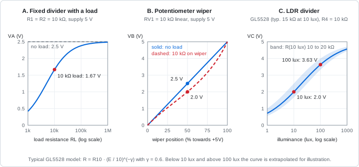
| Plot | Reading |
|---|---|
| A | $V_A$ against load resistance on a log axis. The curve approaches 2.5 V for light loads and falls steeply as the load drops below about 10 kΩ. The marker shows JP1 fitted: 1.67 V |
| B | $V_B$ against wiper position. Solid: a straight line (no load). Dashed: with a 10 kΩ load on the wiper, the curve sags below the line (2.0 V at 50 %) |
| C | $V_C$ against illuminance on a log axis. The solid curve is the typical LDR, and the shaded band covers the 10 kΩ to 20 kΩ spread at 10 lux |
4.2 Response in time
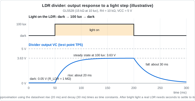
| Time | Event | VC |
|---|---|---|
| 0 to 50 ms | Dark | 0.05 V |
| 50 ms | Light switches to 100 lux | Starts to rise |
| 50 ms to about 200 ms | LDR resistance falls, VC rises with a time constant of about 20 ms |
Reaches 3.63 V |
| 200 ms | Light switches off | Starts to fall |
| 200 ms onwards | LDR resistance recovers, VC falls with a time constant of about 30 ms |
Heads back towards 0.05 V |
The diagram is an illustration: it treats the datasheet response times (about 20 ms rise and 30 ms decay) as first-order time constants. The real part also has a long memory of recent light, so after bright light it needs seconds to settle to its dark resistance. At a multimeter’s reading rate (a few readings per second) these delays are invisible.
5. Schematic
5.1 Symbols and footprints
| Ref | Library symbol | Value | Footprint |
|---|---|---|---|
J1 |
Connector:Conn_01x02_Pin |
Conn_01x02_Pin | Connector_PinHeader_2.54mm:PinHeader_1x02_P2.54mm_Vertical |
R1 |
Device:R |
10k | Resistor_SMD:R_0805_2012Metric |
R2 |
Device:R |
10k | Resistor_SMD:R_0805_2012Metric |
R3 |
Device:R |
10k | Resistor_SMD:R_0805_2012Metric |
R4 |
Device:R |
10k | Resistor_SMD:R_0805_2012Metric |
JP1 |
Jumper:Jumper_2_Open |
Jumper_2_Open | Connector_PinHeader_2.54mm:PinHeader_1x02_P2.54mm_Vertical |
RV1 |
Device:R_Potentiometer |
10k | Potentiometer_THT:Potentiometer_Bourns_3296W_Vertical |
LDR1 |
Device:R_Photo |
GL5528 | OptoDevice:R_LDR_5.1x4.3mm_P3.4mm_Vertical |
TP1 to TP5 |
Connector:TestPoint |
TP1 to TP5 | TestPoint:TestPoint_THTPad_D2.0mm_Drill1.0mm |
| Power | power:+5V, power:GND, power:PWR_FLAG ×2 |
n/a | n/a |
Check the footprints against the datasheets of the parts you buy: lead spacing of the LDR and pin order of the potentiometer. If they differ, choose the matching footprint from the OptoDevice and Potentiometer_THT libraries.
5.2 Nets
| Net | Connections |
|---|---|
+5V |
J1-1, R1-1, RV1-3, LDR1-1, TP1 |
GND |
J1-2, R2-2, R3-2, RV1-1, R4-2, TP2 |
VA |
R1-2, R2-1, JP1-1, TP3 |
LOAD |
JP1-2, R3-1 |
VB |
RV1-2, TP4 |
VC |
LDR1-2, R4-1, TP5 |
5.3 Design decisions
- Net labels
VA,VB,VCandLOADname the important nodes. The test points attach to those nets. LDR1on the supply side,R4on the ground side.VCthen rises with light. Swapping the two would makeVCfall with light.RV1end 3 on+5V, end 1 onGND. Turning the shaft towards end 3 raisesVB. Check your part’s datasheet for the rotation direction, and swap pins 1 and 3 in the schematic if you want the opposite.- A jumper instead of a switch.
JP1keeps the board simple and shows how a jumper changes a circuit without soldering. PWR_FLAGon+5VandGNDtells ERC that both nets are driven by an external supply.TP2(GND) sits next to the signal test points so one black probe lead reaches the reference.
5.4 Schematic conventions
- Signal flows left to right, positive supply at the top, ground at the bottom.
- The three sections are drawn side by side and labelled A, B and C.
- Reference and value fields are visible and not overlapping.
- Schematic grid: 1.27 mm (50 mil).
- The title block is filled in (title, date, revision, author).
6. KiCad configuration
6.1 Project creation
- Create the folder
03-voltage-dividerinside the repository. - In KiCad, choose File → New Project, browse to that folder, name the project
03_voltage_divider, and untick “Create a new folder for the project”.
6.2 Board setup
Import the settings from the previous board: in the PCB editor, open File → Board Setup, click Import Settings from Another Board…, select 02_555_blinker.kicad_pcb, tick the stackup, design rules, net classes and text defaults, and confirm.
| Setting | Value |
|---|---|
| Copper layers | 2, board thickness 1.6 mm, 1 oz copper |
| Minimum clearance | 0.2 mm |
| Minimum track width | 0.2 mm |
| Minimum connection width | 0.2 mm |
| Minimum annular width | 0.15 mm |
| Minimum via diameter | 0.6 mm |
| Copper to hole clearance | 0.3 mm |
| Copper to edge clearance | 0.5 mm |
| Minimum drill size | 0.3 mm |
| Hole to hole clearance | 0.5 mm |
| Silkscreen: minimum clearance / text height / text thickness | 0.15 mm / 1.0 mm / 0.15 mm |
| Net class | Clearance | Track width | Via diameter / drill | Nets |
|---|---|---|---|---|
Default |
0.2 mm | 0.25 mm | 0.6 mm / 0.3 mm | all others |
Power |
0.2 mm | 0.5 mm | 0.8 mm / 0.4 mm | +5V, GND |
These are the same values used for Projects 1 and 2. They are based on typical low-cost 2-layer fab capabilities (see References). Re-check your fab’s current limits before ordering.
6.3 Grid
PCB grid: 0.5 mm for placement, 0.25 mm or 0.1 mm for routing. For the test point row use 5.08 mm.
7. Layout
7.1 Outline
A rectangle on Edge.Cuts, 70 × 40 mm, with 3 mm corner radius. The outline is a single closed shape with no gaps.
7.2 Placement
| Rule | Reason |
|---|---|
| Arrange the three sections side by side, A on the left, B in the middle, C on the right | Matches the schematic and the silkscreen boxes |
J1 at the left edge |
Easy connection of the supply |
Test points TP1 to TP5 in a row along the bottom edge on a 5.08 mm pitch, in the order +5V, GND, VA, VB, VC |
Spaced for multimeter probes and hook clips, and GND sits next to the signals |
RV1 near the top edge, with its adjustment screw facing up |
Screwdriver access |
LDR1 at the right edge, with at least 10 mm of clear space around it |
Nothing may shade the sensor |
Keep tall parts (RV1, about 10 mm) away from LDR1 and never place them on its light side |
A tall neighbour casts a shadow and corrupts the reading |
R1, R2, R3 and JP1 grouped together |
Short connections in section A |
R4 close to LDR1 |
Short VC node |
7.3 Routing
| Rule | Value |
|---|---|
Signal track width (VA, VB, VC, LOAD) |
0.25 mm |
Power track width (+5V, GND) |
0.5 mm |
| Corner angles | 45° or curved, never 90° |
| Copper to board edge | at least 0.5 mm |
| Via size | 0.6 mm pad / 0.3 mm drill |
Keep the measured nodes VA, VB and VC short and away from the +5V track. They carry no current worth speaking of, so they are easy to disturb. After soldering, clean flux residue with isopropyl alcohol, because dirty boards leak and the LDR1 dark-state impedance is high.
7.4 Ground pour and stitching vias
- A
GNDzone on bothF.CuandB.Cu. The bottom layer is kept as a nearly continuous ground plane. R2,R3andR4are surface-mount parts, so their ground pads connect to the top-layer pour. A few stitching vias (0.6 mm / 0.3 mm), roughly every 10 mm to 15 mm, tie the two pours together. Select each via and confirm its net isGND.- Through-hole pads connect to the pour through thermal reliefs.
- Refill zones (press
B) before every DRC run and before plotting.
7.5 Silkscreen
- Reference designators 1.0 mm to 1.5 mm tall, with stroke at least 0.15 mm.
- Three rectangles drawn on
F.Silkscreen(line width 0.15 mm) grouping sections A, B and C, with the titlesA FIXED,B POTandC LDR. - Test point labels
+5V,GND,VA,VB,VCnext to each pad, andLOADnext toJP1. - Pin 1 marked on
J1, the board name, version number, date and author. - No text over pads, and kept at least 0.5 mm from the board edge.
8. Verification
| Check | How | Result |
|---|---|---|
| ERC | Schematic editor → Inspect → Electrical Rules Checker | 0 errors |
| DRC | PCB editor → Inspect → Design Rules Checker | 0 errors, 0 unrouted |
| Board statistics | PCB editor status bar | 22 pads, 6 nets |
| 3D view | PCB editor → View → 3D Viewer (Alt+3) | LDR1 and RV1 orientation correct, nothing shading LDR1 |
| Gerber check | Third-party viewer (KiCad Gerber Viewer, Gerbv, tracespace) | Outline closed, holes aligned, silkscreen clear of pads |
Saved reports are in reports/.
9. Manufacturing outputs
9.1 Gerber plot settings (File → Fabrication Outputs → Gerbers)
| Setting | Value |
|---|---|
| Output directory | fabrication/gerbers |
| Layers | F.Cu, B.Cu, F.Paste, B.Paste, F.Silkscreen, B.Silkscreen, F.Mask, B.Mask, Edge.Cuts |
| Use Protel filename extensions | On |
| Subtract soldermask from silkscreen | On |
| Check zone fills before plotting | On |
| Coordinate format | 4.6, unit mm |
| Use extended X2 format | On |
| Include netlist attributes | On |
| Disable aperture macros | Off |
| Use drill/place file origin | Off |
| Plot drawing sheet | Off |
9.2 Drill file settings
| Setting | Value |
|---|---|
| Drill file format | Excellon |
| Oval holes drill mode | Use alternate drill mode |
| Drill origin | Absolute |
| Drill units | Millimetres |
| Zeros format | Decimal format |
| Map file format (optional) | Gerber |
9.3 Suggested fab order options
| Option | Value |
|---|---|
| Layers | 2 |
| Thickness | 1.6 mm |
| Outer copper weight | 1 oz |
| Surface finish | HASL (lead-free if available) |
| Quantity | Fab minimum |
Verify the generated files in a Gerber viewer, zip the gerbers folder, and upload the zip.
10. Bring-up and testing
10.1 Before powering
- Solder the 0805 resistors first, then the headers, test points, potentiometer and the LDR.
- Check that
RV1andLDR1sit flat and that nothing blocks the light path to the LDR. - With a multimeter in continuity mode, confirm there is no short between
+5VandGND.
10.2 Powered test
Set the multimeter to DC volts. Keep the black probe on TP2 (GND) throughout.
- Leave
JP1open. Apply 5 V toJ1(pin 1 = +5 V, pin 2 = GND). MeasureTP1: this is your actual supply voltage. - Measure
TP3(VA). It should be half the supply. - Fit the shunt on
JP1.TP3should fall to about one third of the supply, 1.67 V at 5.00 V. - Turn
RV1from one end stop to the other while measuringTP4(VB). It should sweep from about 0 V to about the supply voltage. - Measure
TP5(VC) in normal room light. CoverLDR1with a finger: it should fall. Shine a phone torch on it: it should rise. - Calculate the LDR resistance from your readings: $R_{LDR} = 10\ \text{k}\Omega \times (V_{TP1} - V_{TP5}) / V_{TP5}$.
| Measurement | Expected | Measured |
|---|---|---|
Supply at TP1 |
5.0 V (4.75 V to 5.25 V) | |
VA, JP1 open |
half the supply, 2.475 V to 2.525 V at 5.00 V | |
VA, JP1 fitted |
about one third of the supply, 1.645 V to 1.689 V at 5.00 V | |
VB at one end stop |
about 0 V | |
VB at the other end stop |
about the supply voltage | |
VB at mid-travel |
about half the supply | |
VC, finger over LDR (dim) |
low, typically below 1 V | |
VC, normal room light |
roughly 3.5 V to 4.5 V (varies a lot between parts and rooms) | |
VC, phone torch close to LDR |
close to the supply voltage | |
Calculated R_LDR in room light |
about 1 kΩ to 4 kΩ | |
| Supply current | about 1 mA (0.95 mA typical, 1.29 mA maximum) |
10.3 Troubleshooting
| Symptom | Likely cause |
|---|---|
VA reads 0 V or the full supply |
R1 or R2 missing or open, or a solder bridge |
VA with JP1 fitted does not change |
Shunt not making contact, or R3 not soldered |
VB does not change when turning RV1 |
Wiper pin (pin 2) not soldered, or the pot is in the wrong footprint orientation |
VB sweeps the wrong way |
Pot pins 1 and 3 swapped relative to the shaft direction. This is not a fault, and you can swap the end connections if you prefer |
VC stuck near 0 V |
LDR1 open, or R4 open and the LDR in the dark |
VC stuck near the supply |
R4 shorted to the supply, or the LDR is shorted |
| Readings drift or are noisy | Flux residue on the board, or a poor probe contact. Clean with isopropyl alcohol |
VC changes slowly when the light changes |
Normal: the LDR lags by tens of milliseconds and remembers recent light for seconds |
11. Lessons learned
- A voltage divider output is only valid when the load is much larger than its output resistance.
- Measuring a circuit can change it. Check the meter’s input resistance against the circuit’s output resistance.
- Use one standard resistor value across a board where you can, because it simplifies design and purchasing.
- A sensor’s datasheet gives ranges, not exact values. Design for the spread (here 10 kΩ to 20 kΩ at 10 lux), then measure the real part.
- Place test points with probing in mind: a ground point next to the signals saves time.
- Keep the area around an optical sensor clear of tall parts.
12. References
- GL5528 CdS photoresistor datasheet (GL55 series manual), for example the Rapid Electronics copy: https://static.rapidonline.com/pdf/58-0134_v1.pdf
- KiCad documentation: https://docs.kicad.org
- JLCPCB capabilities: https://jlcpcb.com/capabilities/pcb-capabilities
- JLCPCB guide to generating Gerber and drill files in KiCad: https://jlcpcb.com/help/article/how-to-generate-gerber-and-drill-files-in-kicad-7