kicad-learning-path
NPN Transistor Switch


A PN2222A NPN transistor that lets a push-button switch loads up to 75 mA at 5 V, with an LED indicator, a flyback diode and test points on the base and collector. Project 4 of my KiCad learning path: the transistor as a switch, the base resistor, saturation and the flyback diode.
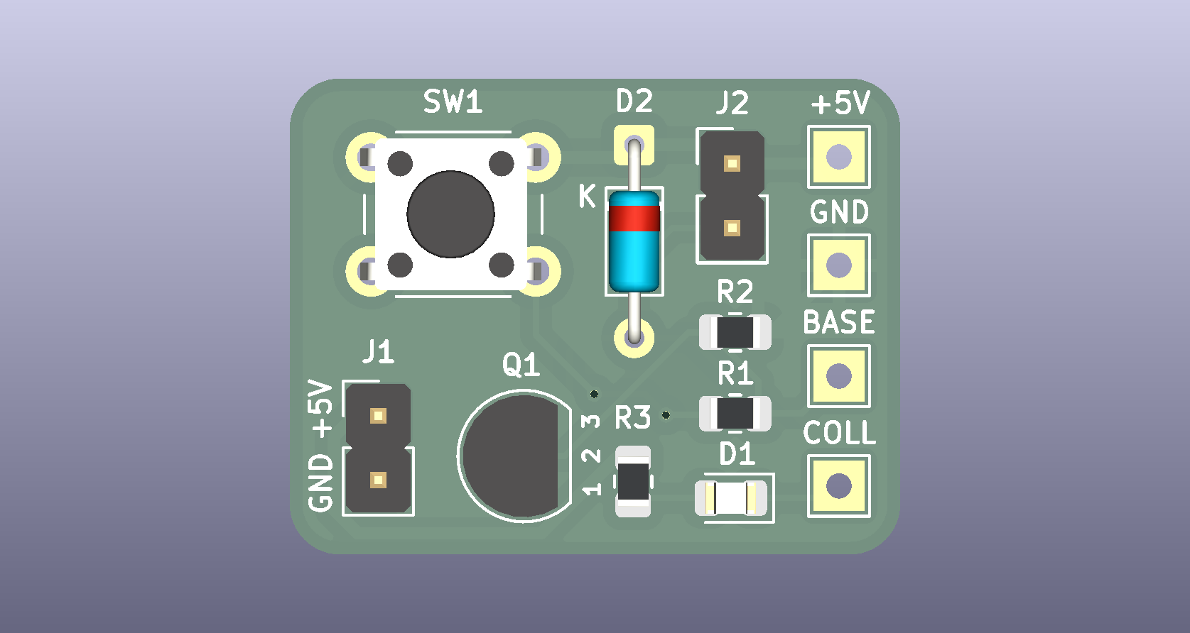
Table of contents
- Overview
- Key specifications
- Gallery
- Switching waveform and saturation curve
- How the circuit works
- Design calculations (summary)
- Purpose of each component
- Bill of materials
- Netlist
- Repository structure
- Getting started
- Testing
- Verification status
- Future improvements
- License
Overview
Project 1 let a button drive an LED directly. A button and its contacts cannot carry much current, and a microcontroller pin can supply only a few milliamps. A transistor solves this: a small base current controls a much larger collector current, so a weak signal can switch a real load.
| Part of the circuit | What it demonstrates |
|---|---|
Q1 with base resistor R1 |
A transistor driven hard into saturation so it acts like a closed switch |
R2 |
A pull-down resistor that keeps the transistor firmly off when the button is released |
D1 and R3 |
An indicator LED that shows the switch is on, and adds a second load |
J2 and D2 |
An external load connector, and a flyback diode that protects the transistor from inductive spikes |
TP3 and TP4 |
Test points to measure the base and collector voltages |
New ideas compared with Project 3:
- The NPN transistor, its three regions (cutoff, active, saturation) and its datasheet limits
- Choosing a base resistor with a “forced gain” of 10 so saturation is guaranteed
- Switching a load on its low side
- Inductive loads and the flyback diode
- A net class for a net that carries real current (
COLL) - A switching waveform in the documentation
The full engineering write-up (theory, derivations, tolerance analysis, KiCad configuration, layout rules, test procedure) is in docs/DESIGN_NOTES.md.
Key specifications
| Parameter | Value |
|---|---|
| Supply voltage | 5 V DC via J1 |
| Transistor | PN2222A (NPN, TO-92), 40 V, 600 mA |
Switched load at J2 |
up to 75 mA at 5 V, low-side switched |
| Indicator LED current | 8.5 mA |
| Base drive current | 10.4 mA (forced gain 7.6 at the 68 Ω reference load, never above 8.75) |
| Saturation voltages | VCE(sat) about 0.2 V, VBE about 0.9 V |
| Flyback clamp voltage | about 5.9 V (supply plus one diode drop) |
| Supply current | about 0 mA released, 19 mA pressed with no external load, about 90 mA with the 68 Ω reference load |
| Board layers | 2 |
| Board thickness | 1.6 mm |
| Copper weight | 1 oz (35 µm) |
| Board size | 60 × 40 mm |
| Components | 13 (9 circuit parts and 4 test points) |
| Pads / nets | 25 / 6 |
| Design tool | KiCad 10.0.x |
| ERC / DRC | 0 errors / 0 errors |
Gallery
Schematic
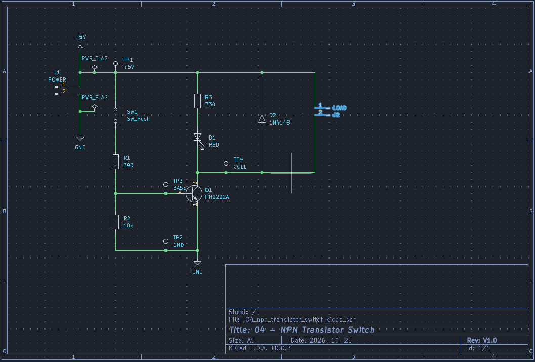
Full-size PDF: docs/schematic.pdf
PCB layout
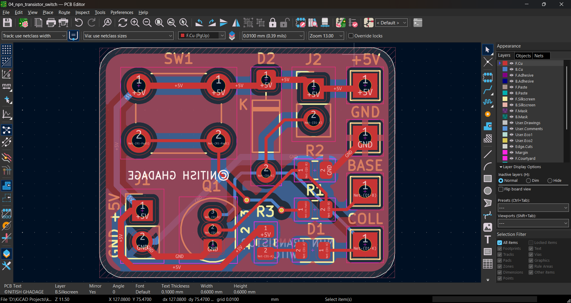
3D views
| Top | Bottom |
|---|---|
|
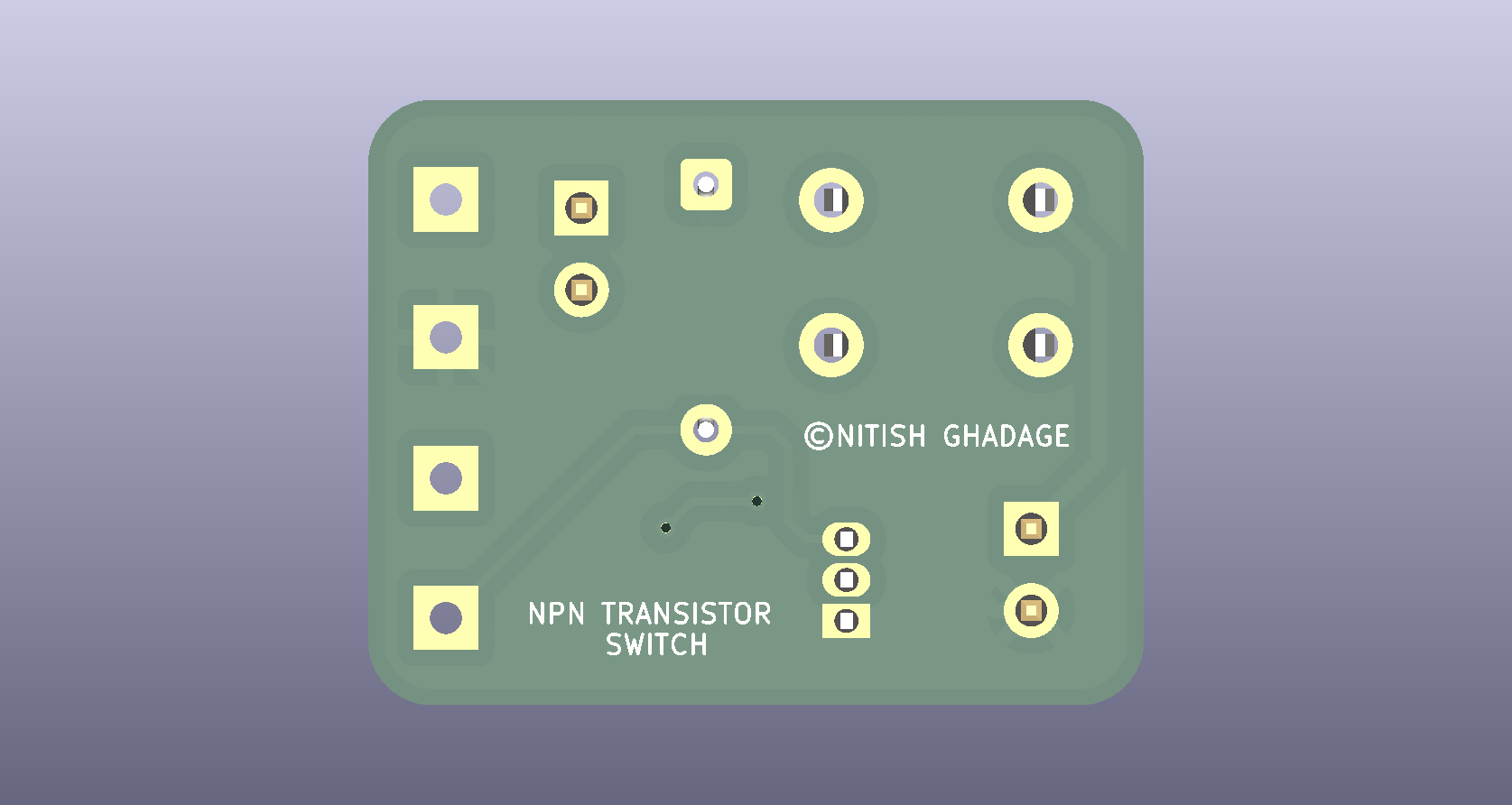 |
Switching waveform and saturation curve
Switching waveform
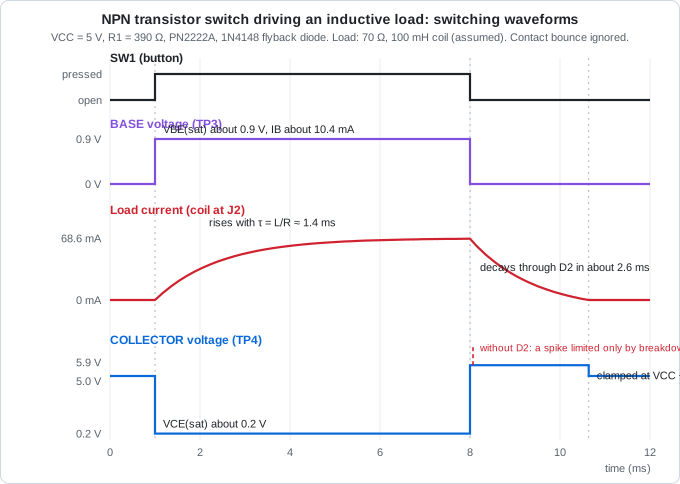
| Time | Event | Base (TP3) |
Collector (TP4) |
Load current |
|---|---|---|---|---|
| Before press | Button open, R2 holds the base low |
0 V | 5.0 V (coil connected) | 0 |
| Button pressed | R1 supplies 10.4 mA of base current |
about 0.9 V | falls to about 0.2 V | rises with τ = L/R |
| Pressed, settled | Transistor saturated | about 0.9 V | about 0.2 V | 68.6 mA for a 70 Ω coil |
| Button released | Base current stops, the transistor turns off | 0 V | jumps to 5.9 V, clamped by D2 |
decays through D2 in about 2.6 ms |
| After decay | Coil current has reached zero | 0 V | back to 5.0 V | 0 |
The diagram assumes a coil of 70 Ω and 100 mH, which is an illustration. The red dashed line marks what would happen without D2: the collector voltage would be limited only by breakdown.
Saturation curve
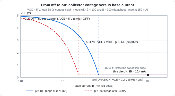
The curve shows the collector voltage against base current for a 68 Ω load. With little base current the transistor is off (cutoff). As the current rises, the collector voltage falls along a slope set by the gain (active region). Beyond a small current it flattens at about 0.2 V (saturation). This circuit drives the base with 10.4 mA, 15 to 44 times the amount needed to just reach saturation, so the switch is firmly on whatever the gain of the individual transistor.
How the circuit works
 +5V ──┬── SW1 ── R1 390 Ω ──┬── Q1 base
       │                      R2 10k to GND
       ├── R3 330 Ω ── D1 LED ──┐
       ├── J2 pin 1 (load +) ─┬─┤
       └── D2 cathode         │ ├── Q1 collector (COLL) ── J2 pin 2 (load −)
                              └─┘     D2 anode
                          Q1 emitter ── GND
- Released.
R2holds the base at 0 V. Without about 0.6 V between base and emitter the transistor conducts nothing, so the LED and the external load are off. - Pressed.
SW1connects+5VtoR1. About 10.4 mA flows into the base. That small current allows a much larger collector current: the LED branch (8.5 mA) and the external load (up to 75 mA) pull the collector down to about 0.2 V, so the load sees almost the full 5 V. - Released again. The base current stops and the transistor switches off. If the load is a coil (relay, solenoid, motor), its current cannot stop at once and tries to push the collector voltage up.
D2conducts and gives that current a path back to the supply, clamping the collector at about 5.9 V.
The transistor sits on the low side of the load: the load connects between +5V and the collector, and the transistor connects the load to ground.
Design calculations (summary)
Base resistor. Choose a collector current and a forced gain of 10 (the condition under which the datasheet guarantees VCE(sat)):
Actual base current:
\[I_{R1} = \frac{5.0\ \text{V} - 0.9\ \text{V}}{390\ \Omega} = 10.51\ \text{mA} \qquad I_B = I_{R1} - \frac{0.9\ \text{V}}{10\ \text{k}\Omega} = 10.42\ \text{mA}\]Collector current (68 Ω reference load plus the LED branch):
\[I_L = \frac{5.0 - 0.2}{68\ \Omega} = 70.6\ \text{mA} \qquad I_{LED} = \frac{5.0 - 2.0 - 0.2}{330\ \Omega} = 8.5\ \text{mA} \qquad I_C = 79.1\ \text{mA}\]Forced gain: $I_C / I_B = 79.1 / 10.42 = 7.6$, below 10, so the transistor is saturated.
| Quantity | Value |
|---|---|
| Worst-case forced gain (tolerances, same supply voltage) | 8.75 at 4.75 V, 8.54 at 5.25 V |
| Largest total collector current with guaranteed saturation | 10 × 8.89 mA = 88.9 mA |
Q1 power |
25.2 mW (38 mW worst case), against 625 mW |
R1 power |
43.1 mW (56 mW worst case), against about 125 mW |
| Flyback clamp | 5.0 V + 0.9 V = 5.9 V, far below the transistor’s 40 V rating |
The full derivation, datasheet values, tolerance cases and the flyback analysis are in docs/DESIGN_NOTES.md.
Purpose of each component
| Ref | Value | Purpose |
|---|---|---|
J1 |
2-pin header | Brings in 5 V (pin 1) and ground (pin 2) |
SW1 |
6 mm tactile push-button | The input: closing it sends current into the base |
R1 |
390 Ω, 1 % | Sets the base current to 10.4 mA, enough to saturate Q1 with margin |
R2 |
10 kΩ, 1 % | Pull-down: keeps the base at 0 V when SW1 is open, so stray pickup below 60 µA cannot turn Q1 on |
Q1 |
PN2222A | The switch. 40 V, 600 mA, gain 100 to 300 at 150 mA |
R3 |
330 Ω, 1 % | Limits the indicator LED current to 8.5 mA |
D1 |
Red LED, 0805 | Indicator: lights when Q1 is on |
J2 |
2-pin header | Connector for an external load (up to 75 mA at 5 V). Pin 1 is +5V, pin 2 is the switched side |
D2 |
1N4148 | Flyback diode across J2: carries the coil current when Q1 turns off, and protects Q1 |
TP1 |
Test point | +5V |
TP2 |
Test point | GND, the reference for all measurements |
TP3 |
Test point | BASE: measure VBE and the base current through R1 |
TP4 |
Test point | COLL: measure VCE(sat) and the flyback clamp |
Bill of materials
| Ref | Qty | Value | Footprint | Description |
|---|---|---|---|---|
J1 |
1 | Conn_01x02_Pin | PinHeader_1x02_P2.54mm_Vertical |
2-pin header, 5 V in |
J2 |
1 | Conn_01x02_Pin | PinHeader_1x02_P2.54mm_Vertical |
2-pin header, external load |
SW1 |
1 | SW_Push | SW_PUSH_6mm |
6 mm tactile push-button |
R1 |
1 | 390 Ω | R_0805_2012Metric |
Base resistor, 1 % |
R2 |
1 | 10 kΩ | R_0805_2012Metric |
Base pull-down, 1 % |
R3 |
1 | 330 Ω | R_0805_2012Metric |
LED resistor, 1 % |
Q1 |
1 | PN2222A | TO-92_Inline |
NPN transistor, pin order E-B-C |
D1 |
1 | RED | LED_0805_2012Metric |
Red LED, 0805 |
D2 |
1 | 1N4148 | D_DO-35_SOD27_P7.62mm_Horizontal |
Small-signal diode, flyback |
TP1 to TP4 |
4 | TestPoint | TestPoint_THTPad_D2.0mm_Drill1.0mm |
Through-hole test points |
The same list is available as CSV in fabrication/bom.csv.
Netlist
| Net | Connections |
|---|---|
+5V |
J1-1, SW1-1, R3-1, J2-1, D2 cathode, TP1 |
GND |
J1-2, Q1 emitter, R2-2, TP2 |
BTN |
SW1-2, R1-1 |
BASE |
R1-2, R2-1, Q1 base, TP3 |
COLL |
Q1 collector, J2-2, D2 anode, D1 cathode, TP4 |
LEDA |
R3-2, D1 anode |
Repository structure
This project lives in the 04-npn-transistor-switch/ folder of the kicad-learning-path repository.
04-npn-transistor-switch/
├── README.md
├── 04_npn_transistor_switch.kicad_pro     KiCad project file
├── 04_npn_transistor_switch.kicad_sch     Schematic
├── 04_npn_transistor_switch.kicad_pcb     PCB layout
├── fabrication/
│   ├── gerbers/                           Gerber and drill files
│   ├── 04_npn_transistor_switch_gerbers.zip
│   └── bom.csv
└── docs/
    ├── DESIGN_NOTES.md                    Full engineering documentation
    ├── schematic.pdf
    ├── images/                            Waveform, saturation curve, screenshots, renders
    └── reports/                           ERC and DRC reports
Getting started
Open the project
- Install KiCad 10.
- Clone or download this repository.
- Open
04-npn-transistor-switch/04_npn_transistor_switch.kicad_proin KiCad. The project uses only the standard KiCad libraries.
Rebuild the manufacturing files
- Open the PCB editor and run Inspect → Design Rules Checker. It should report 0 errors.
- Open File → Fabrication Outputs → Gerbers and Generate Drill Files. The exact settings are listed in
docs/DESIGN_NOTES.md. - Zip the output folder.
Order the PCB
Upload fabrication/04_npn_transistor_switch_gerbers.zip to a PCB fabricator. Suggested options for a low-cost fab: 2 layers, 1.6 mm, 1 oz copper, HASL finish.
Testing
Step-by-step measurements, expected values and a troubleshooting table are in docs/DESIGN_NOTES.md. In short: apply 5 V and press SW1. The LED lights, TP3 reads about 0.9 V, and TP4 falls to a few tenths of a volt. Connect a 68 Ω, 1 W resistor to J2 as a test load and check that TP4 stays below 0.3 V.
Verification status
| Check | Result |
|---|---|
| Electrical Rules Check (ERC) | 0 errors |
| Design Rules Check (DRC) | 0 errors, 0 unrouted nets |
| Gerber viewer check | Passed |
| Physical board built and tested | Not yet |
Reports: docs/reports/
Future improvements
- Replace
SW1with a logic input so a microcontroller can drive the base (a 3.3 V signal gives a base current of about 6 mA, soR1would need to be smaller) - Switch the same load with an N-MOSFET and compare the results (Project 12)
- Add a second stage to drive larger loads
- Add mounting holes
License
Released under the MIT License.
Author: Nitish Ghadage · GitHub