kicad-learning-path
Design Notes: Diode Power Entry and 5 V Linear Regulator
Revision 1.0 · KiCad 10.0.x · Last updated: 2026-10-24
This document records every engineering decision behind the board: the theory of the linear regulator and of heat, the calculations and tolerance analysis, the operating-area and power-budget diagrams, the KiCad configuration, the layout rules, the verification results, the manufacturing settings and the test procedure.
Contents
- Requirements
- Electronics background
- Calculations
- Operating area and power budget
- Schematic
- KiCad configuration
- Layout
- Verification
- Manufacturing outputs
- Bring-up and testing
- Lessons learned
- References
1. Requirements
| # | Requirement |
|---|---|
| R1 | Accept a 9 V battery or a DC supply from 7.6 V to 12 V through a screw terminal |
| R2 | Survive a reversed supply connection without damage |
| R3 | Deliver a regulated 5 V within 4.75 V to 5.25 V |
| R4 | Deliver 300 mA in free air (input up to 10 V, 40 °C ambient), and 500 mA with a heatsink (input up to 12 V) |
| R5 | Keep the regulator’s junction temperature below 125 °C in every rated condition |
| R6 | Always satisfy the regulator’s minimum load current |
| R7 | Show that 5 V is present, with an indicator LED |
| R8 | Let the input, the protected input, the output and ground be measured at test points |
| R9 | Hand-solderable parts (through-hole and 0805 SMD) |
| R10 | 2-layer board that a low-cost fab can build without special options |
| R11 | Zero ERC errors and zero DRC errors |
2. Electronics background
2.1 Why regulate
Batteries sag as they discharge, bench supplies are set to whatever the user dials, and wall adapters vary with load. Electronics usually needs a fixed voltage, so a regulator sits between the source and the circuit and holds the output constant while the input and the load change.
2.2 How a linear regulator works
A linear regulator contains four blocks:
| Block | Function |
|---|---|
| Voltage reference | A stable internal voltage that does not depend on the input |
| Error amplifier | Compares a fraction of the output with the reference |
| Pass transistor | A transistor in series with the load, controlled by the amplifier |
| Protection | Current limiting, safe-area protection and thermal shutdown |
If the output rises, the amplifier turns the pass transistor down. If it falls, the amplifier turns it up. The pass transistor behaves like an automatic variable resistor in series with the load, and it drops the surplus voltage:
\[V_{drop} = V_{in} - V_{out} \qquad P_{reg} = (V_{in} - V_{out}) \times I_{out} + V_{in} \times I_q\]The second term is the quiescent current $I_q$ the regulator itself consumes. All of this power turns into heat inside the package.
2.3 Dropout voltage
The pass transistor needs some voltage across it to work. The minimum difference between input and output is the dropout voltage. For the L7805C the datasheet gives 2 V at 1 A and 25 °C, and the dropout is smaller at lower currents. Below this, the regulator can no longer hold 5 V and the output follows the input down.
\[V_{in,regulator} \ge V_{out} + V_{dropout} = 5\ \text{V} + 2\ \text{V} = 7\ \text{V}\]2.4 Efficiency
The current into a linear regulator equals the current out plus the quiescent current. Ignoring the latter, the best possible efficiency is simply the voltage ratio:
\[\eta \le \frac{V_{out}}{V_{in}} \qquad \frac{5}{9} = 55.6\ \% \qquad \frac{5}{12} = 41.7\ \%\]Efficiency does not improve with load current. It is a fixed penalty of the topology. Switching regulators (Project 13) avoid it.
2.5 Heat, thermal resistance and junction temperature
Heat flows from the silicon (the junction) to the surrounding air through a chain of thermal resistances, measured in °C per watt:
| Symbol | Path | L78 TO-220 value |
|---|---|---|
| $R_{\theta JC}$ | Junction to case | 5 °C/W |
| $R_{\theta CS}$ | Case to heatsink (thermal pad or paste) | about 1 °C/W (assumed) |
| $R_{\theta SA}$ | Heatsink to ambient | depends on the heatsink |
| $R_{\theta JA}$ | Junction to ambient, no heatsink | 50 °C/W |
The junction temperature is:
\[T_J = T_A + P \times R_{\theta JA}\]With a heatsink, the total resistance is $R_{\theta JC} + R_{\theta CS} + R_{\theta SA}$. To find the heatsink needed for a given power:
\[R_{\theta SA} \le \frac{T_{J,max} - T_A}{P} - R_{\theta JC} - R_{\theta CS}\]The L78C operating junction range is 0 °C to 125 °C. The regulator also has internal thermal shutdown, which turns the output off if it overheats, but a design must never rely on it.
2.6 Reverse-polarity protection and the cost of a diode drop
Plugging a supply in backwards would push current the wrong way through the regulator and capacitors, destroying electrolytic capacitors in particular. A series diode passes current in the correct direction and blocks it in the reverse direction. Its cost is a forward voltage drop and the power it wastes:
\[P_{diode} = V_F \times I\]| Diode type | Forward drop | Consequence |
|---|---|---|
| Silicon (for example 1N4007) | about 1 V | Higher loss and a higher minimum input voltage |
| Schottky (1N5819) | 0.6 V maximum at 1 A, lower at lower currents | Less heat and more headroom |
A Schottky diode has a metal-semiconductor junction with a lower forward drop, at the price of a higher reverse leakage (up to 1 mA at 25 °C for the 1N5819 at its full rated reverse voltage).
2.7 Capacitors around a regulator
| Part | Type | Role |
|---|---|---|
C1, input |
100 µF electrolytic | A reservoir that supplies sudden current demands, so the input does not sag through the supply’s wiring resistance and inductance |
C2, input |
1 µF ceramic X7R | Handles fast changes. It must be right at the regulator’s input pin |
C3, output |
100 nF ceramic X7R | Handles fast load changes and keeps the output quiet |
C4, output |
100 µF electrolytic | A reservoir that improves the response to load steps |
Why two types in parallel? An electrolytic capacitor stores a lot of charge but responds slowly, because of its internal resistance and inductance. A ceramic capacitor stores little but responds quickly. Together they cover both timescales.
Things to remember:
- Electrolytic capacitors are polarised. A reversed electrolytic can fail violently.
- Voltage rating. Choose at least twice the working voltage.
- Ceramic DC-bias loss. Class-2 ceramics (X7R) lose capacitance when they carry DC voltage, so a larger nominal value gives margin.
- Temperature. Electrolytic capacitors age faster when hot (a common rule of thumb is that life halves for every 10 °C increase), so they must be kept away from the regulator and the diode.
The L78 datasheet advises bypassing the regulator input when it is far from the supply filter, with a capacitor of 0.33 µF or larger that has low impedance at high frequency, mounted with the shortest possible leads directly across the input terminals. It also notes that no output capacitor is needed for stability, but that one improves the transient response.
2.8 Minimum load current
A fixed regulator such as the L7805 needs a small minimum load to regulate properly. The datasheet states that the minimum load current for regulation is 5 mA. With no load, the output could drift upwards. The power LED branch (9.1 mA) guarantees this minimum.
2.9 Datasheet limits
L7805C (STMicroelectronics L78 series, DS0422, TO-220):
| Parameter | Value |
|---|---|
| Output voltage at 25 °C ($V_I$ = 10 V, $I_O$ = 500 mA) | 4.8 V / 5 V / 5.2 V (min / typ / max) |
| Output voltage over line, load and temperature ($I_O$ 5 mA to 1 A, $V_I$ 7 V to 18 V) | 4.75 V to 5.25 V |
| Line regulation, $V_I$ 7 V to 25 V | 3 mV typical, 100 mV maximum |
| Line regulation, $V_I$ 8 V to 12 V | 1 mV typical, 50 mV maximum |
| Load regulation, 5 mA to 1.5 A | 100 mV maximum |
| Load regulation, 250 mA to 750 mA | 50 mV maximum |
| Quiescent current | 8 mA maximum |
| Quiescent current change | 0.5 mA (load 5 mA to 1 A), 0.8 mA ($V_I$ 7 V to 23 V) |
| Output noise (10 Hz to 100 kHz) | 40 µV per volt of output |
| Supply voltage rejection ($V_I$ 8 V to 18 V, 120 Hz) | 62 dB minimum |
| Dropout voltage ($I_O$ = 1 A, 25 °C) | 2 V |
| Output resistance (1 kHz) | 17 mΩ |
| Short circuit current ($V_I$ = 35 V) | 0.75 A |
| Short circuit peak current | 2.2 A |
| Output voltage drift | −1.1 mV/°C |
| Maximum input voltage (output 5 V to 18 V) | 35 V |
| Operating junction temperature (L78C) | 0 °C to 125 °C |
| Thermal resistance, TO-220: junction to case / junction to ambient | 5 °C/W / 50 °C/W |
| Minimum load current for regulation | 5 mA |
1N5819 (Diodes Incorporated DS23001 and equivalents):
| Parameter | Value |
|---|---|
| Repetitive peak reverse voltage | 40 V |
| Average forward current | 1 A |
| Peak forward surge (8.3 ms) | 25 A |
| Forward voltage at 1 A | 0.60 V maximum (0.90 V at 3 A) |
| Reverse current at 25 °C, rated reverse voltage | 1 mA maximum |
| Package | DO-41, the stripe marks the cathode |
3. Calculations
3.1 Inputs
| Symbol | Meaning | Value | Source |
|---|---|---|---|
| $V_{in}$ | Supply voltage at J1 |
7.6 V to 12 V, 9 V nominal | Requirement R1 |
| $V_{out}$ | Regulated output | 5.0 V | L7805C |
| $V_F$ | Diode drop | 0.45 V typical (assumed between the datasheet points), 0.6 V maximum | 1N5819 datasheet |
| $I_q$ | Regulator quiescent current | 8 mA (datasheet maximum, used for a conservative power figure) | L7805C |
| $I_{LED}$ | Power LED branch | 9.09 mA (see 3.7) | Design |
| $R_{\theta JA}$ | Junction to ambient, no heatsink | 50 °C/W | L78 datasheet |
| $R_{\theta JC}$ | Junction to case | 5 °C/W | L78 datasheet |
| $T_{J,max}$ | Maximum junction temperature | 125 °C | L78C datasheet |
| $T_A$ | Ambient temperature | 25 °C (lab) and 40 °C (warm enclosure) | Requirement |
3.2 Minimum input voltage
The regulator’s input must be at least 7 V (the lowest input in the datasheet’s regulation specification, equal to 5 V plus the 2 V dropout). The diode takes up to 0.6 V:
\[V_{in,min} = 7.0\ \text{V} + 0.6\ \text{V} = 7.6\ \text{V}\]With a typical drop of 0.45 V the limit is 7.45 V. A 9 V battery is considered flat at 7.6 V.
3.3 Regulator power and junction temperature
The load current in the table is the current into J2. The total output current is that plus the 9.09 mA LED branch.
Worked example, 9 V in and 300 mA load:
\[V_{raw} = 8.55\ \text{V} \qquad I_{out} = 0.3091\ \text{A} \qquad P_{reg} = 3.55 \times 0.3091 + 8.55 \times 0.008 = 1.166\ \text{W}\] \[T_J = 25 + 1.166 \times 50 = 83\ ^\circ\text{C} \qquad T_{case} = T_J - P \times R_{\theta JC} = 83 - 1.166 \times 5 = 77\ ^\circ\text{C}\]Vin |
Load | Vraw |
P_reg |
ΔT (50 °C/W) |
T_J at 25 °C |
T_J at 40 °C |
Verdict |
|---|---|---|---|---|---|---|---|
| 9 V | 0 mA | 8.55 V | 0.10 W | 5 °C | 30 °C | 45 °C | Fine |
| 9 V | 100 mA | 8.55 V | 0.46 W | 23 °C | 48 °C | 63 °C | Fine |
| 9 V | 300 mA | 8.55 V | 1.17 W | 58 °C | 83 °C | 98 °C | Fine (design rating) |
| 9 V | 500 mA | 8.55 V | 1.88 W | 94 °C | 119 °C | 134 °C | Heatsink needed at 40 °C |
| 12 V | 100 mA | 11.55 V | 0.81 W | 40 °C | 65 °C | 80 °C | Fine |
| 12 V | 300 mA | 11.55 V | 2.12 W | 106 °C | 131 °C | 146 °C | Heatsink needed |
| 12 V | 500 mA | 11.55 V | 3.43 W | 171 °C | 196 °C | 211 °C | Heatsink needed |
| 7.6 V | 300 mA | 7.15 V | 0.72 W | 36 °C | 61 °C | 76 °C | Fine |
3.4 Maximum load against input voltage
Rearranging the power equation for the maximum current at a given power limit $P_{max} = (T_{J,max} - T_A) / R_{\theta total}$:
\[I_{load,max} = \frac{P_{max} - V_{raw} \times 0.008}{V_{raw} - 5.0} - 0.00909\]Vin |
Free air, 25 °C ($P_{max}$ = 2.00 W) | Free air, 40 °C ($P_{max}$ = 1.70 W) | Heatsink 18 °C/W, 40 °C ($P_{max}$ = 3.54 W) |
|---|---|---|---|
| 7.6 V | 895 mA | 755 mA | above 1 A |
| 8 V | 752 mA | 634 mA | |
| 9 V | 535 mA | 451 mA | 969 mA |
| 10 V | 414 mA | 348 mA | |
| 11 V | 336 mA | 282 mA | |
| 12 V | 282 mA | 236 mA | 518 mA |
The design rating follows from this table: 300 mA in free air up to 10 V input at 40 °C ambient (the limit there is 348 mA), and 500 mA up to 12 V with a heatsink of 18 °C/W or better. The plot in section 4 shows the same data.
3.5 Heatsink selection
\[R_{\theta SA} \le \frac{125 - 40}{P} - 5 - 1\]| Condition | P_reg |
Required $R_{\theta SA}$ |
|---|---|---|
| 9 V in, 500 mA out | 1.88 W | 39 °C/W or better (a very small clip-on heatsink) |
| 12 V in, 500 mA out | 3.43 W | 18.8 °C/W or better, so choose 18 °C/W or better |
With an 18 °C/W heatsink at 12 V and 500 mA: $T_J = 40 + 3.43 \times (5 + 1 + 18) = 122\ ^\circ\text{C}$, just under the limit. For more margin, use a lower input voltage or a larger heatsink.
3.6 Efficiency and the power budget
\[\eta = \frac{V_{out} \times I_{out}}{V_{in} \times (I_{out} + I_q)}\]| Operating point | Input power | Load power | Regulator heat | Diode heat | Efficiency |
|---|---|---|---|---|---|
| 9 V, 100 mA | 1.05 W | 0.55 W | 0.46 W | 0.05 W | 52 % |
| 9 V, 300 mA | 2.85 W | 1.55 W | 1.17 W | 0.14 W | 54 % |
| 9 V, 500 mA | 4.65 W | 2.55 W | 1.88 W | 0.23 W | 55 % |
| 12 V, 300 mA | 3.81 W | 1.55 W | 2.12 W | 0.14 W | 41 % |
More than half of the input power is wasted in every case. That is the price of a linear regulator’s simplicity.
3.7 Power LED and the minimum load
\[I_{LED} = \frac{V_{out} - V_F}{R_1} = \frac{5.0\ \text{V} - 2.0\ \text{V}}{330\ \Omega} = 9.09\ \text{mA}\]| Quantity | Value |
|---|---|
R1 power |
27.3 mW (about 125 mW rating for 0805) |
D2 power |
18.2 mW |
Minimum load required by U1 |
5 mA |
| Margin | 9.09 mA is 1.8 times the minimum |
3.8 Reverse-polarity diode
| Quantity | Value |
|---|---|
| Power at 300 mA (typical drop 0.45 V) | 0.14 W |
| Power at 500 mA (typical drop 0.45 V) | 0.23 W |
| Worst case, 0.6 V at 0.5 A | 0.30 W |
| Current rating margin | 0.5 A against 1 A average and 25 A surge |
| Reverse voltage margin | 12 V maximum input against 40 V rating |
| Reverse leakage at a reversed connection | 1 mA maximum at 25 °C at the full 40 V |
| Compared with a silicon diode (about 1 V) | Silicon would lose about 0.32 W at 300 mA and raise the minimum input to about 8 V |
3.9 Capacitor selection
| Part | Value | Reasoning |
|---|---|---|
C1 |
100 µF, 25 V | A 300 mA demand lasting 100 µs takes 30 µC, which droops 100 µF by $Q/C = 0.3$ V. The 25 V rating is 2.2 times the highest working voltage (11.55 V) |
C2 |
1 µF, 50 V X7R | The datasheet asks for 0.33 µF or larger. A 1 µF part keeps well above that after DC-bias loss at 8.5 V |
C3 |
100 nF, 50 V X7R | The datasheet’s test value for the output capacitor |
C4 |
100 µF, 16 V | The 16 V rating is 3.2 times the 5 V working voltage |
3.10 Regulation accuracy
| Effect | Datasheet limit | At this design |
|---|---|---|
| Output voltage tolerance | 4.75 V to 5.25 V over all conditions (4.8 V to 5.2 V at 25 °C) | 5 V ±5 % |
| Line regulation, 8 V to 12 V input | 50 mV maximum | 1 % of 5 V at most |
| Load regulation, 250 mA to 750 mA | 50 mV maximum | 1 % of 5 V at most |
| Supply voltage rejection, 120 Hz | 62 dB minimum | 1 V of ripple on the input appears as 0.79 mV on the output |
| Output resistance, 1 kHz | 17 mΩ | A 300 mA load step changes the output by about 5 mV |
| Output noise | 40 µV per volt of output | about 200 µV for 5 V |
| Temperature drift | −1.1 mV/°C | about −0.11 V over a 100 °C swing |
3.11 Test loads
Resistors that draw current from the 5 V output generate real heat. Choose a power rating of at least twice the dissipation.
| Load resistor | Current at 5 V | Dissipation | Minimum power rating |
|---|---|---|---|
| 100 Ω | 50 mA | 0.25 W | 0.5 W |
| 47 Ω | 106 mA | 0.53 W | 1 W |
| 33 Ω | 152 mA | 0.76 W | 2 W |
| 22 Ω | 227 mA | 1.14 W | 3 W |
| 15 Ω | 333 mA | 1.67 W | 5 W |
| 10 Ω | 500 mA | 2.50 W | 5 W (10 W for long tests) |
3.12 Component purposes
| Ref | Value | Purpose |
|---|---|---|
J1 |
Screw terminal | Supply input |
D1 |
1N5819 | Reverse-polarity protection |
U1 |
L7805CV | 5 V regulation |
C1 |
100 µF, 25 V | Input reservoir |
C2 |
1 µF, 50 V | Input high-frequency bypass |
C3 |
100 nF, 50 V | Output high-frequency bypass |
C4 |
100 µF, 16 V | Output reservoir |
R1 |
330 Ω | LED current limit |
D2 |
Red LED | Power indicator and minimum load |
J2 |
Header | 5 V output |
TP1 to TP4 |
Test points | VIN, VRAW, +5V, GND |
4. Operating area and power budget
4.1 Dropout and thermal limits
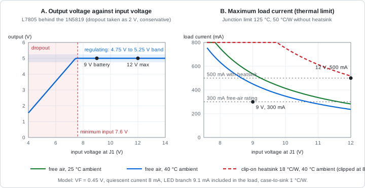
| Plot | Reading |
|---|---|
| A | Output voltage against input voltage at J1. The curve flattens at 5 V once the input is high enough (the shaded band is the 4.75 V to 5.25 V tolerance). To the left of 7.6 V the regulator is in dropout and the output follows the input down. The 2 V dropout figure is for 1 A, so the real knee at lower currents is a little further left |
| B | Maximum load current against input voltage for three cooling conditions. The curves fall as the input rises, because the same current produces more heat. The marked points are the design ratings |
4.2 Where the power goes
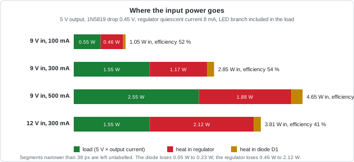
Each bar is the input power split into three parts: useful load power (green), heat in the regulator (red) and heat in the diode (orange). The red segment grows quickly with input voltage: compare 9 V and 12 V at the same 300 mA.
4.3 No timing diagram
This board is a DC circuit with no periodic signals, so the roadmap’s extra for this project is the voltage and power budget above rather than a timing diagram. The only time-dependent effects are the capacitors’ response to load steps (a few millivolts, see 3.10) and the slow warming of the regulator, which takes minutes.
5. Schematic
5.1 Symbols and footprints
| Ref | Library symbol | Value | Footprint |
|---|---|---|---|
J1 |
Connector:Screw_Terminal_01x02 |
VIN | TerminalBlock:TerminalBlock_bornier-2_P5.08mm |
J2 |
Connector:Conn_01x02_Pin |
5V_OUT | Connector_PinHeader_2.54mm:PinHeader_1x02_P2.54mm_Vertical |
D1 |
Diode:1N5819 |
1N5819 | Diode_THT:D_DO-41_SOD81_P10.16mm_Horizontal |
U1 |
Regulator_Linear:L7805 |
L7805CV | Package_TO_SOT_THT:TO-220-3_Vertical |
C1 |
Device:CP |
100uF 25V | Capacitor_THT:CP_Radial_D6.3mm_P2.50mm |
C2 |
Device:C |
1uF | Capacitor_SMD:C_0805_2012Metric |
C3 |
Device:C |
100nF | Capacitor_SMD:C_0805_2012Metric |
C4 |
Device:CP |
100uF 16V | Capacitor_THT:CP_Radial_D6.3mm_P2.50mm |
R1 |
Device:R |
330 | Resistor_SMD:R_0805_2012Metric |
D2 |
Device:LED |
RED | LED_SMD:LED_0805_2012Metric |
TP1 to TP4 |
Connector:TestPoint |
TP1 to TP4 | TestPoint:TestPoint_THTPad_D2.0mm_Drill1.0mm |
| Power | power:+5V, power:GND, power:PWR_FLAG ×2 |
n/a | n/a |
The L7805 symbol has pin 1 as input, pin 2 as ground and pin 3 as output, which matches the TO-220 package. Check the diameter and lead spacing of your electrolytic capacitors against the footprint.
5.2 Nets
| Net | Connections |
|---|---|
VIN |
J1-1, D1 anode, TP1 |
VRAW |
D1 cathode, C1 +, C2-1, U1-1, TP2 |
+5V |
U1-3, C3-1, C4 +, R1-1, J2-1, TP3 |
GND |
J1-2, U1-2, C1 −, C2-2, C3-2, C4 −, D2 cathode, J2-2, TP4 |
LEDA |
R1-2, D2 anode |
5.3 Design decisions
D1in series on the positive rail. Anode toVIN, cathode toVRAW. If it were reversed, the circuit would never power up.C2atU1pin 1. In the schematic it is drawn next to the regulator, and in the layout it must be physically there.- Output capacitors present although the regulator does not need them for stability. They improve transient response.
- No protection diode across the regulator. The datasheet calls for one only with high-capacitance loads and outputs above 6 V, so it is omitted at 5 V.
PWR_FLAGonVRAWand onGND. The regulator’s input pin is a power input that nothing on theVRAWnet drives, because the diode’s pins are passive. The same is true ofGND. APWR_FLAGon each of those two nets tells ERC that an external supply drives them. The+5Vnet needs no flag, becauseU1’s output pin is a power output.- Net labels
VIN,VRAW,LEDAname the important nodes. The output net uses the+5Vpower symbol. - The LED sits on the regulated output, so it shows that regulation is working, not just that the input is connected.
5.4 Schematic conventions
- Signal flows left to right, positive supply at the top, ground at the bottom.
- The input sections (
J1,D1,C1,C2) are on the left, the regulator in the middle, and the output sections (C3,C4,R1,D2,J2) on the right. - Reference and value fields are visible and not overlapping.
- Schematic grid: 1.27 mm (50 mil).
- The title block is filled in (title, date, revision, author).
6. KiCad configuration
6.1 Project creation
- Create the folder
05-linear-regulatorinside the repository. - In KiCad, choose File → New Project, browse to that folder, name the project
05_linear_regulator, and untick “Create a new folder for the project”.
6.2 Board setup
Import the settings from the previous board: in the PCB editor, open File → Board Setup, click Import Settings from Another Board…, select 04_npn_transistor_switch.kicad_pcb, tick the stackup, design rules, net classes and text defaults, and confirm.
| Setting | Value |
|---|---|
| Copper layers | 2, board thickness 1.6 mm, 1 oz copper |
| Minimum clearance | 0.2 mm |
| Minimum track width | 0.2 mm |
| Minimum connection width | 0.2 mm |
| Minimum annular width | 0.15 mm |
| Minimum via diameter | 0.6 mm |
| Copper to hole clearance | 0.3 mm |
| Copper to edge clearance | 0.5 mm |
| Minimum drill size | 0.3 mm |
| Hole to hole clearance | 0.5 mm |
| Silkscreen: minimum clearance / text height / text thickness | 0.15 mm / 1.0 mm / 0.15 mm |
6.3 Net classes (new in this project)
This board carries up to 0.5 A on its supply path, so it gets a wider class. Open Board Setup → Design Rules → Net Classes, add a class called Supply, and edit the patterns so that no net matches two classes.
| Net class | Clearance | Track width | Via diameter / drill | Net patterns |
|---|---|---|---|---|
Default |
0.2 mm | 0.25 mm | 0.6 mm / 0.3 mm | all others (LEDA) |
Power |
0.2 mm | 0.5 mm | 0.8 mm / 0.4 mm | GND (remove +5V and COLL from this class) |
Supply |
0.2 mm | 1.0 mm | 0.8 mm / 0.4 mm | VIN, VRAW, +5V |
Under Pre-defined Sizes, add a track width of 1.0 mm.
Why 1.0 mm. The IPC-2221 estimate for a 1 oz outer-layer track at a 10 °C rise is about 0.9 A for 0.25 mm, 1.4 A for 0.5 mm and 2.4 A for 1.0 mm. The supply path carries at most about 0.5 A, so 0.5 mm would be enough electrically. The wider track costs nothing, lowers the voltage drop, and is easier to connect to the large pads of the terminal block and regulator. Ground is mostly a copper pour, so its tracks only need to reach the pour.
6.4 Grid
PCB grid: 0.5 mm for placement, 0.25 mm or 0.1 mm for routing. For the test point row use 5.08 mm.
7. Layout
7.1 Outline
A rectangle on Edge.Cuts, 70 × 45 mm, with 3 mm corner radius. The outline is a single closed shape with no gaps.
7.2 Placement
| Rule | Reason |
|---|---|
Power flows left to right: J1, D1, C1, U1, C4, J2 |
Short supply path, matching the schematic |
J1 at the left edge, J2 at the right edge |
Short, separate input and output paths |
C2 touching U1 pin 1, C3 touching U1 pin 3 |
The datasheet asks for the shortest possible leads at the input, and the output capacitor works best close to the pin |
U1 near the top edge, with the tab facing outwards |
Room for a clip-on heatsink and airflow |
Keep a 20 × 15 mm area around U1’s tab free of parts |
Heatsink and airflow clearance |
C1, C4 and the LED at least 10 mm from U1 and D1 |
Electrolytic capacitors age faster when hot |
R1 and D2 at the bottom of the board |
Away from the heat |
TP1 to TP4 in a row along the bottom edge on a 5.08 mm pitch, in the order VIN, VRAW, +5V, GND |
Probe-friendly, with GND last |
7.3 Routing
| Rule | Value |
|---|---|
VIN, VRAW, +5V track width |
1.0 mm (the Supply net class applies this) |
GND |
0.5 mm tracks to the pour (the Power net class) |
LEDA track width |
0.25 mm |
| Corner angles | 45° or curved, never 90° |
| Copper to board edge | at least 0.5 mm |
| Via size | 0.6 mm pad / 0.3 mm drill (0.8 mm / 0.4 mm in the Supply and Power classes) |
TO-220 pads. The TO-220-3_Vertical footprint has its pads on a 2.54 mm pitch with a gap of about 0.64 mm between them. A 1.0 mm track cannot pass between the pads, so route the supply tracks to the pads from outside. Only a 0.25 mm track fits between them.
The input path. Run VIN, then D1, then VRAW in a straight line, so that the large input current does not mix with the sensitive output path.
7.4 Ground pour and stitching vias
- A
GNDzone on bothF.CuandB.Cu. The bottom layer is kept as a nearly continuous ground plane. - The surface-mount ground pads (
C2,C3) connect to the top-layer pour. A few stitching vias (0.6 mm / 0.3 mm), roughly every 10 mm to 15 mm, tie the two pours together. Select each via and confirm its net isGND. - Through-hole pads connect to the pour through thermal reliefs.
- A copper pour next to
U1helps spread a little heat, but it is not a replacement for a heatsink. - Refill zones (press
B) before every DRC run and before plotting.
7.5 Silkscreen
- Reference designators 1.0 mm to 1.5 mm tall, with stroke at least 0.15 mm.
J1:+at pin 1 and−at pin 2, with the label7.6-12V IN.J2:5V OUT.- The cathode stripe of
D1shown clearly, and the+mark ofC1andC4. - A label
HOTnearU1. - Pin labels for
U1:IN,GND,OUT. - Test point labels
VIN,VRAW,+5V,GND. - The board name, version, date and author.
- No text over pads, and kept at least 0.5 mm from the board edge.
8. Verification
| Check | How | Result |
|---|---|---|
| ERC | Schematic editor → Inspect → Electrical Rules Checker | 0 errors |
| DRC | PCB editor → Inspect → Design Rules Checker | 0 errors, 0 unrouted |
| Board statistics | PCB editor status bar | 25 pads, 5 nets |
| 3D view | PCB editor → View → 3D Viewer (Alt+3) | Orientation of D1, C1, C4 and U1 correct, space for a heatsink |
| Gerber check | Third-party viewer (KiCad Gerber Viewer, Gerbv, tracespace) | Outline closed, holes aligned, silkscreen clear of pads |
Saved reports are in reports/.
9. Manufacturing outputs
9.1 Gerber plot settings (File → Fabrication Outputs → Gerbers)
| Setting | Value |
|---|---|
| Output directory | fabrication/gerbers |
| Layers | F.Cu, B.Cu, F.Paste, B.Paste, F.Silkscreen, B.Silkscreen, F.Mask, B.Mask, Edge.Cuts |
| Use Protel filename extensions | On |
| Subtract soldermask from silkscreen | On |
| Check zone fills before plotting | On |
| Coordinate format | 4.6, unit mm |
| Use extended X2 format | On |
| Include netlist attributes | On |
| Disable aperture macros | Off |
| Use drill/place file origin | Off |
| Plot drawing sheet | Off |
9.2 Drill file settings
| Setting | Value |
|---|---|
| Drill file format | Excellon |
| Oval holes drill mode | Use alternate drill mode |
| Drill origin | Absolute |
| Drill units | Millimetres |
| Zeros format | Decimal format |
| Map file format (optional) | Gerber |
9.3 Suggested fab order options
| Option | Value |
|---|---|
| Layers | 2 |
| Thickness | 1.6 mm |
| Outer copper weight | 1 oz |
| Surface finish | HASL (lead-free if available) |
| Quantity | Fab minimum |
Verify the generated files in a Gerber viewer, zip the gerbers folder, and upload the zip.
10. Bring-up and testing
10.1 Safety
- The regulator, the heatsink and the load resistors get hot. At 9 V in and 300 mA out, the regulator’s case reaches about 77 °C. Do not hold it. Use an infrared thermometer or a thermocouple.
- Never use a supply above 12 V on this board without recalculating the heat.
- Check the polarity of
C1andC4before powering up. - Use a bench supply with a current limit if you have one.
10.2 Before powering
- Solder the 0805 parts first, then
D1, the headers, test points and terminal block, then the electrolytic capacitors and finallyU1(with its heatsink, if used). - Check the orientation of
D1(stripe towardsU1),D2(cathode towardsGND),C1andC4(stripe side toGND) andU1(tab towards the board edge). - With a multimeter in continuity mode, confirm there is no short between
+5VandGND, and none betweenVINandGND.
10.3 Reverse-polarity test (do this first)
- Set a bench supply to 9 V with a current limit of 50 mA.
- Connect it reversed to
J1. - Measure
TP3: it should be about 0 V. The supply current should be well below 1 mA (the diode’s leakage). - Disconnect, then reconnect correctly.
10.4 Powered test
Set the multimeter to DC volts. Keep the black probe on TP4 (GND).
- Apply 9 V to
J1. MeasureTP1(VIN) andTP2(VRAW). The difference is the diode drop. It must be 0.6 V or less. - Measure
TP3: about 5 V, within 4.8 V to 5.2 V. The LED lights. - Connect a test load from the table in 3.11 between the pins of
J2. Start with 100 Ω, then 47 Ω, then 22 Ω. At each step, wait a minute and recordTP3andTP2. - With 22 Ω (227 mA),
TP3should change by 50 mV or less compared with no load. - Dropout test (optional): with a 47 Ω load and an adjustable supply, slowly reduce
TP1from 9 V. The output should hold up to about 7.6 V, then begin to fall. - Thermal test: run at 9 V and 300 mA (15 Ω, 5 W load) for 5 minutes and measure the regulator’s case temperature with an infrared thermometer. Expect about 75 °C at 25 °C ambient.
| Measurement | Expected | Measured |
|---|---|---|
Reverse connection: TP3 and supply current |
about 0 V, well below 1 mA | |
TP1 (VIN) |
9.0 V (or your supply setting) | |
TP1 − TP2 (diode drop) |
0.6 V or less (about 0.2 V to 0.5 V depending on load) | |
TP3, no load |
4.8 V to 5.2 V | |
TP3, 22 Ω load |
within 50 mV of the no-load value | |
| LED | On | |
| Supply current, no load | about 9 mA (LED) plus up to 8 mA quiescent, so about 15 mA | |
| Regulator case temperature, 9 V and 300 mA | about 75 °C at 25 °C ambient | |
Regulation starts to fail at TP1 of about |
7.6 V (or lower at light load) |
10.5 Troubleshooting
| Symptom | Likely cause |
|---|---|
| No output, no LED | D1 fitted backwards (stripe towards J1), no input, or U1 fitted wrongly |
Output stuck near 0 V and U1 gets hot |
A short on the output, or C3/C4 reversed or shorted |
| Output low (about 4 V) at heavy load | The input is too low: the regulator is in dropout. Check TP2 |
| Output drifts up with no load | Load below the 5 mA minimum: the LED branch is missing or open (R1, D2) |
| Regulator too hot to touch at 300 mA | Normal at 9 V (about 77 °C). Add a heatsink, lower the input voltage or reduce the load |
| Regulator shuts down repeatedly | Overheating: thermal shutdown. Reduce the load or add a heatsink |
| Output noisy or oscillating | C2 missing, or too far from U1’s input pin |
| An electrolytic capacitor bulges or smells | Reversed polarity or too high a voltage: switch off immediately and replace |
| Input supply collapses when the load is connected | Supply or battery cannot deliver the current, or the wiring is too thin |
11. Lessons learned
- A linear regulator turns surplus voltage into heat. Always calculate $(V_{in} - V_{out}) \times I$ before choosing the input voltage.
- Efficiency is fixed by the voltage ratio. A lower input voltage gives a cooler, more efficient regulator, as long as it stays above the dropout limit.
- The diode that protects against reversed polarity costs voltage headroom and power. A Schottky diode costs less than a silicon one.
- Read the minimum load current on a regulator’s datasheet. A power LED makes a convenient minimum load.
- Put the input bypass capacitor at the regulator’s pin, not somewhere nearby.
- Keep electrolytic capacitors away from heat sources.
- Check every rating against the worst case, not the typical case, and test with real resistors that can survive the heat.
12. References
- STMicroelectronics, L78 Positive voltage regulator ICs datasheet (DS0422): https://www.st.com/resource/en/datasheet/l78.pdf
- Diodes Incorporated, 1N5817 - 1N5819, 1.0 A Schottky Barrier Rectifier datasheet (DS23001), for example this copy: https://mrsdprojects.ri.cmu.edu/2025teamb/wp-content/uploads/sites/84/2025/05/diodes.pdf
- KiCad documentation: https://docs.kicad.org
- JLCPCB capabilities: https://jlcpcb.com/capabilities/pcb-capabilities
- JLCPCB guide to generating Gerber and drill files in KiCad: https://jlcpcb.com/help/article/how-to-generate-gerber-and-drill-files-in-kicad-7