kicad-learning-path
LED + Push-Button PCB


A fully documented KiCad 10 project: a 5 V push-button that lights a red LED through a current-limiting resistor. Project 1 of my KiCad learning path, from basic electronics to advanced PCB design.
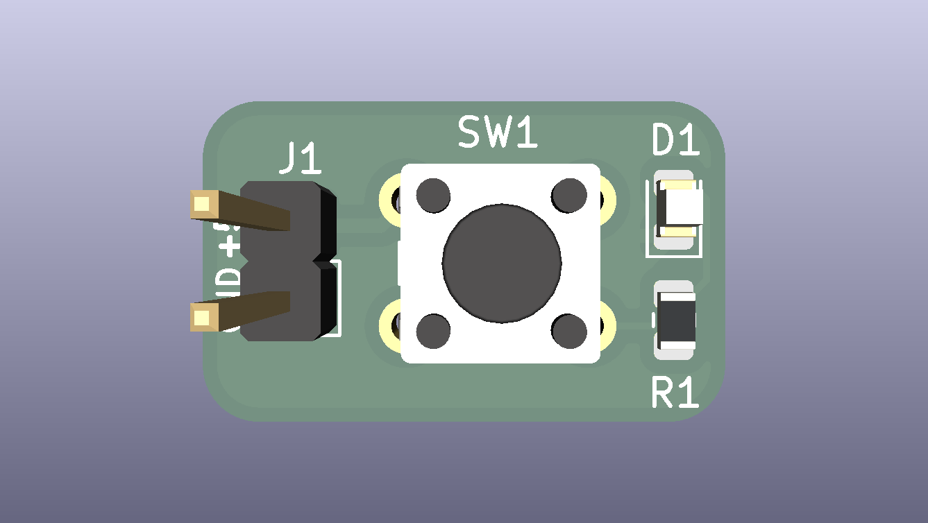
Table of contents
- Overview
- Key specifications
- Gallery
- How the circuit works
- Design calculations (summary)
- Bill of materials
- Netlist
- Repository structure
- Getting started
- Testing
- Verification status
- Future improvements
- Learning-path roadmap
- License
Overview
This board is deliberately simple so that the complete professional PCB workflow is covered end to end:
- Electronics fundamentals and component calculation
- Schematic capture with power flags and a clean ERC
- Footprint assignment
- Board setup: stackup, design constraints, net classes
- Placement, routing and copper pour
- DRC, 3D check and Gerber verification
- Manufacturing file export for a low-cost 2-layer fab
What it does: a 5 V supply is connected to header J1. While push-button SW1 is held down, current flows through resistor R1 and LED D1, and the LED lights. R1 limits the current to about 9 mA.
The full engineering write-up (theory, derivations, KiCad configuration, layout rules, manufacturing settings) is in docs/DESIGN_NOTES.md.
Key specifications
| Parameter | Value |
|---|---|
| Supply voltage | 5 V DC (via J1) |
| LED current (nominal) | ≈ 9.1 mA |
| Current-limit resistor | 330 Ω, 0805, 1 % |
| LED | Red, 0805, forward voltage ≈ 2.0 V |
| Board layers | 2 |
| Board thickness | 1.6 mm |
| Copper weight | 1 oz (35 µm) |
| Board size | 18.750 × 11.480 mm |
| Components | 4 (J1, SW1, R1, D1) |
| Pads / nets / vias | 10 / 4 / 0 |
| Minimum track / clearance | 0.2 mm / 0.2 mm |
| Design tool | KiCad 10.0.x |
| ERC / DRC | 0 errors / 0 errors |
Gallery
Schematic
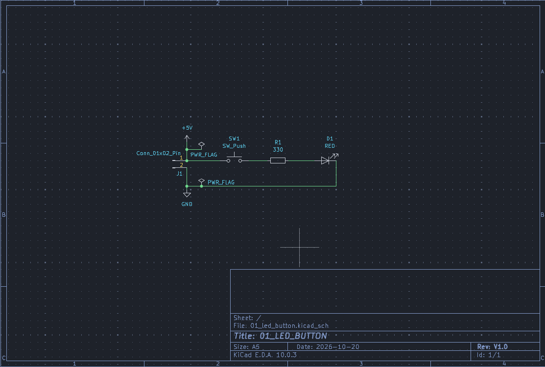
Full-size PDF: docs/schematic.pdf
PCB layout
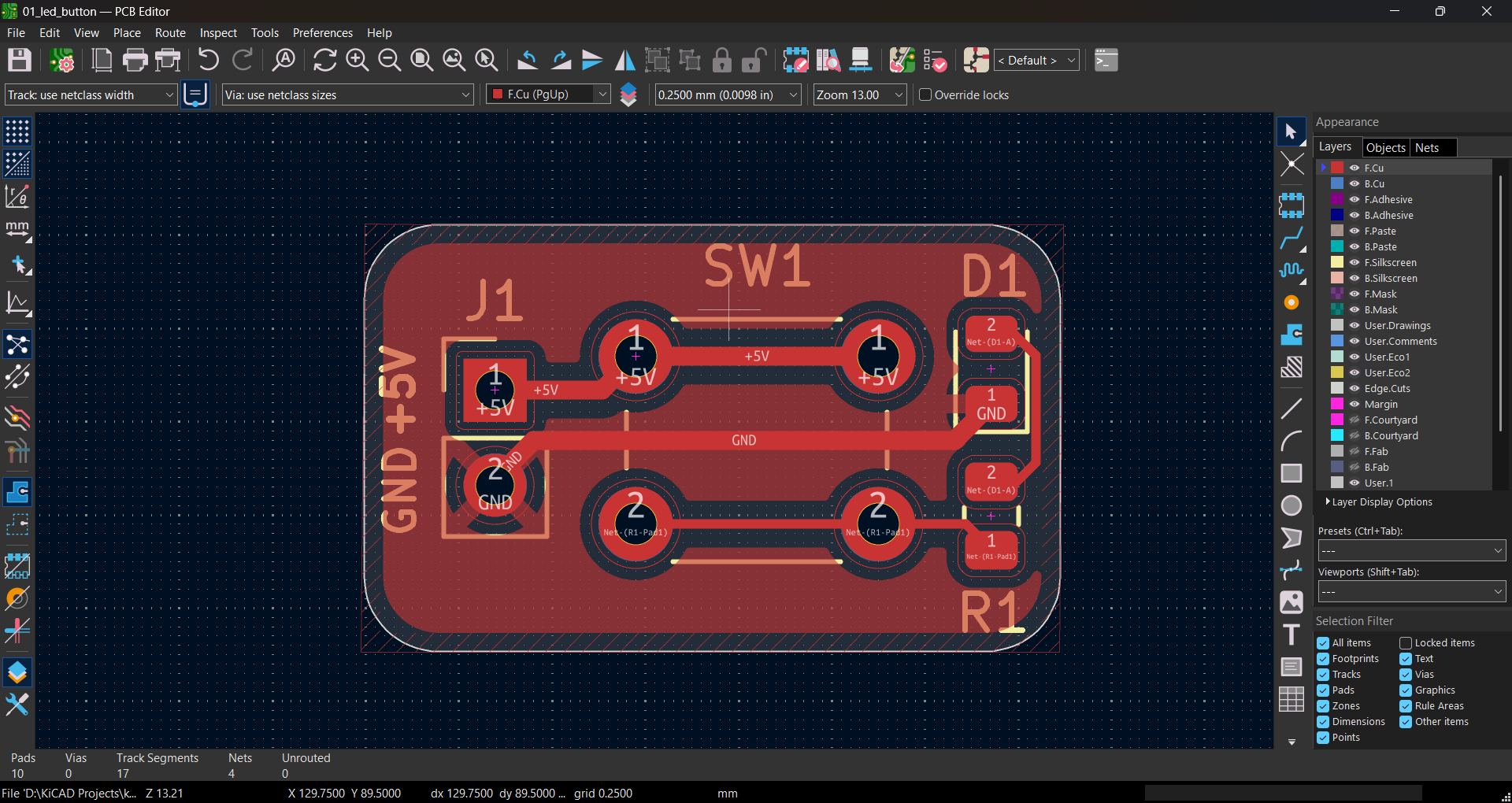
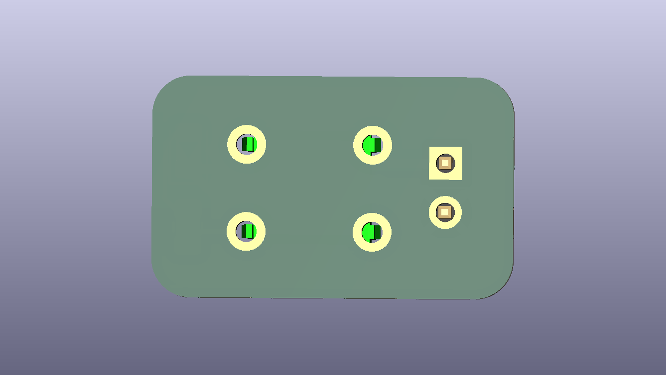
3D views
| Top | Bottom |
|---|---|
|
 |
How the circuit works
+5V ──► SW1 (push button) ──► R1 (330 Ω) ──► D1 (red LED) ──► GND
J1brings in 5 V on pin 1 and ground on pin 2.SW1is normally open. Pressing it completes the loop.R1drops the surplus voltage so the LED current is safe.D1conducts only in the direction of the triangle (anode to cathode) and lights up.- The same current flows through every part, because they are in series.
Design calculations (summary)
Ohm’s law:
\[V = I \times R\]Resistor value for a target LED current:
\[R = \frac{V_S - V_F}{I_F} = \frac{5.0\ \text{V} - 2.0\ \text{V}}{10\ \text{mA}} = 300\ \Omega \;\rightarrow\; \text{330}\ \Omega\ \text{(standard E12 value)}\]Actual current with the standard value:
\[I = \frac{V_S - V_F}{R} = \frac{3.0\ \text{V}}{330\ \Omega} \approx 9.09\ \text{mA}\]Power:
\[P = V \times I = I^2 R\]| Element | Voltage drop | Current | Power |
|---|---|---|---|
R1 (330 Ω) |
3.0 V | 9.09 mA | 27.3 mW (rating of 0805: about 125 mW) |
D1 (red LED) |
≈ 2.0 V | 9.09 mA | 18.2 mW |
SW1 (closed) |
≈ 0 V | 9.09 mA | ≈ 0 mW |
| Total from supply | 5.0 V | 9.09 mA | 45.5 mW |
Worst-case analysis (supply ±5 %, resistor ±1 %, LED forward voltage 1.8 V to 2.2 V) gives a current between 7.65 mA and 10.56 mA, which is safe for the LED and the resistor. The full derivation is in docs/DESIGN_NOTES.md.
Bill of materials
| Ref | Qty | Value | Footprint | Description |
|---|---|---|---|---|
J1 |
1 | Conn_01x02_Pin | PinHeader_1x02_P2.54mm_Vertical |
2-pin 2.54 mm header (5 V in) |
SW1 |
1 | SW_Push | SW_PUSH_6mm |
6 mm tactile push-button |
R1 |
1 | 330 Ω | R_0805_2012Metric |
Resistor, 1 %, 1/8 W |
D1 |
1 | RED | LED_0805_2012Metric |
Red LED, 0805 |
The same list is available as CSV in fabrication/bom.csv.
Netlist
| Net | Connections |
|---|---|
+5V |
J1 pin 1, SW1 pin 1 |
Net-(R1-Pad1) |
SW1 pin 2, R1 pin 1 |
Net-(D1-A) |
R1 pin 2, D1 anode |
GND |
D1 cathode, J1 pin 2 |
Repository structure
kicad-learning-path/
├── README.md                    Index of all projects
├── LICENSE
├── .gitignore
└── 01-led-button/               This project
    ├── README.md                You are here
    ├── 01_led_button.kicad_pro  KiCad project file
    ├── 01_led_button.kicad_sch  Schematic
    ├── 01_led_button.kicad_pcb  PCB layout
    ├── fabrication/
    │   ├── gerbers/             Gerber and drill files
    │   ├── 01_led_button_gerbers.zip
    │   └── bom.csv
    └── docs/
        ├── DESIGN_NOTES.md      Full engineering documentation
        ├── schematic.pdf
        ├── images/              Screenshots and 3D renders
        └── reports/             ERC and DRC reports
Getting started
Open the project
- Install KiCad 10.
- Clone or download the
kicad-learning-pathrepository. - Open
01-led-button/01_led_button.kicad_proin KiCad. The project uses only the standard KiCad libraries.
Rebuild the manufacturing files
- Open the PCB editor and run Inspect → Design Rules Checker. It should report 0 errors.
- Open File → Fabrication Outputs → Gerbers and Generate Drill Files. The exact settings are listed in
docs/DESIGN_NOTES.md. - Zip the output folder.
Order the PCB
Upload fabrication/01_led_button_gerbers.zip to a PCB fabricator. Suggested options for a low-cost fab: 2 layers, 1.6 mm, 1 oz copper, HASL finish.
Testing
Bring-up procedure and expected measurements are in docs/DESIGN_NOTES.md. In short: apply 5 V, press SW1, and the LED lights; the voltage across R1 should read about 3.0 V.
Verification status
| Check | Result |
|---|---|
| Electrical Rules Check (ERC) | 0 errors |
| Design Rules Check (DRC) | 0 errors, 0 unrouted nets |
| Gerber viewer check | Passed |
| Physical board built and tested | Not yet |
Reports: docs/reports/
Future improvements
- Add reverse-polarity protection on
J1 - Add mounting holes
- Reduce silkscreen text size and keep it clear of the board edge
- Add a second LED as a power indicator
- Replace the header with a USB-C connector (see Project 4)
Learning-path roadmap
| # | Project | Status |
|---|---|---|
| 1 | Push-button LED board | Done |
| 2 | 555 timer LED blinker | Planned |
| 3 | Transistor/MOSFET driver | Planned |
| 4 | USB-C to 3.3 V power board | Planned |
| 5 | Microcontroller board | Planned |
| 6 | Advanced capstone | Planned |
License
Released under the MIT License. Replace with a hardware license such as CERN-OHL-P-2.0 if you prefer.
Author: Nitish Ghadage · GitHub